bremenpl
Member level 3

Hello there,
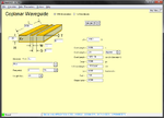
I have a question regarding calculating track width and gaps on the side for 4 layer PCB board, in order to maintain 50 ohm impedance for it. The term I have come across for calling this is "Coplanar waveguide". My problem is, that I need to calculate the widths for 4 layer PCB board, and every source i refer to offers calculation for a single trace with only one power plane underneath. For example AppCAD:

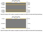
In my application, where I want to make a PCB for a GSM module, the producer provided some examples of PCB stacks, for both 2 and 4 layer PCB:

From this i understand that calculation for 2 and 4 layer board differs, but there is no explanation in the datasheet.
How can I calculate the Coplanar waveguide for a 4 layer PCB (Assuming both planes are GND)? I would really appreciate all help.
I have a question regarding calculating track width and gaps on the side for 4 layer PCB board, in order to maintain 50 ohm impedance for it. The term I have come across for calling this is "Coplanar waveguide". My problem is, that I need to calculate the widths for 4 layer PCB board, and every source i refer to offers calculation for a single trace with only one power plane underneath. For example AppCAD:

In my application, where I want to make a PCB for a GSM module, the producer provided some examples of PCB stacks, for both 2 and 4 layer PCB:

From this i understand that calculation for 2 and 4 layer board differs, but there is no explanation in the datasheet.
How can I calculate the Coplanar waveguide for a 4 layer PCB (Assuming both planes are GND)? I would really appreciate all help.


