Continue to Site

Welcome to EDAboard.com

Welcome to our site! EDAboard.com is an international Electronics Discussion Forum focused on EDA software, circuits, schematics, books, theory, papers, asic, pld, 8051, DSP, Network, RF, Analog Design, PCB, Service Manuals... and a whole lot more! To participate you need to register. Registration is free. Click here to register now.

Virtual ground mid-rail LM386 for low voltage projects.

voxmagna

Newbie level 6
Newbie level 6
Joined
Apr 19, 2020
Messages
14
Helped
0
Reputation
0
Reaction score
0
Trophy points
1
Activity points
173
I often need to split voltage rails for a center rail virtual ground cheap and simple. I'm working with op amp circuits running from battery 4-6 Volts. I took several different op amps from my components stock, bread boarded split rail circuits and learned a lot:

1. The output current can be just a few mA, or some opamps can do 30mA.
2. Some op amps are unstable with a capacitor load on the split rail output
3. The output current into a resistor load isn't always symmetrical sinking to ground or sourcing current from the supply rail.
4. The quiescent current draw of some opamps can be over 3mA, too high for low power battery designs.
5. Adding a BJT output driver with diodes and resistors for more currrent, increases the complexity and parts count.

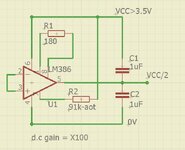
I've tested an unconventional design using an LM386 audio amp IC. It's not an op amp in the normal sense and only has a gain of x20, but it can drive 8 ohm mini speakers or headphones with capacitor loads. It's an old chip with not much in it, but easily sourced cheap. It's capable of X200 gain but that's a.c gain and I wanted higher d.c gain for rail spliting to hold the rail voltage constant at VCC/2 up to 100mA output.

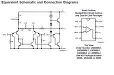
I studied the LM386 architcture and bread boarded it as a rail splitter, testing with a dvm, 'scope for noise, capacitor loads and resistors. Without any aditional parts, it would rail split but had a -250mV offset from center and some voltage variation with resistor test loads when sinking and sourcing current up to 150mA. I studied the LM386 nternal schematic and calculated I could replace the gain capacitor on pins 1 & 8 with a 180 ohm resistor to increase gain from x20 to X100. The fixed offset voltage of VCC/2 -250mV was still present, but I could correct this with an external resistor 91k on pin 7. All my practical tests seem to show this works with 5 parts. Can anybody see the downside because I've not seen anybody do this? Thanks
 

Attachments

  • LM386 Schematic.jpg
    LM386 Schematic.jpg
    163.9 KB · Views: 47
  • My LM386 rail splitter.jpg
    My LM386 rail splitter.jpg
    143.6 KB · Views: 50
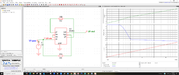
Rough sim :

1731013987832.png


Since inputs not tied to fdbk they sit at ~ ground due to internal pull downs. So
rail is not getting split 1:1


Regards, Dana.
 

Attachments

  • 1731013819924.png
    1731013819924.png
    260.4 KB · Views: 27
I think you might find R divider parallel with
C divider, adequate as long as the divider R
isn't pushed much by Iib. Forget the op amp.
 
Alternate configuration, ramping load R from 5 to 500 ohms -

1731014981290.png


Stability may be another matter.
 
How much is your load, Rl? This affects load regulation error, as error = Rs for the split rail controls the error roughly by Rs/(Rs+Rl)*Vcc
The LM386 Quiescent Current Drain: 4 to 8 mA

The advantage of compensated BJT Op Amps is that they can drive high C loads, CMOS OA's cannot.
The Rs output impedance is reduced by the excess gain so if Rout (open loop) is 300ohms and excess gain is 10k, then the Zout is 300 /10k until current limit is exceeded.
 
Thanks for all your replies. I've met and tried simulations on the internet in the past and found they didn't always tie up in practice. I've built and measured the schematic I posted and it would be interesting to see a simulation that proves what I measured is possible? Dannadakk, when you posted your simulation did you build the diagram from the LM386 schematic or use a generic or library op amp? Every measurement I've made showed I can get a stable mid rail from a 6V supply (I've adjusted it higher and lower) and whilst still supporting a 100-150mA load. It also worked with a large 220uF capacitor on the load tied either to ground, VCC or both. I haven't tried several LM386s from different manufacturers. The only unstable operation I had was when VCC was reduced below 3.5V which I expected and there was complete output cliff edge drop out, but that low voltage is pretty extreme. With a dc gain of only X100 I wasn't expecting instability because the LM386 a.c gain is claimed to be stable at X200.

Can anybody with an LM386 try what I've done in practice and tell me their result, it only takes a few minutes to assemble? I don't use SIM. The LM386 internal architecture isn't like a normal op amp. It's designed for single rail operation with - input pin 2 grounded, when it's output pin 5 sits at half rail (as measured). Here's a link to an article I found helpful because it explains circuit gain and how I arrived at a feedback resistor value of 180 ohms.


Tony, yes I've learned BJTs are better than OA's for rail splitting although I was surprised the TL07 series OAs I tried could drive 30mA at low rail voltage, even with some load capacitance. But have a look at the LM386 architecture explained in the link. The output stage is what you might build using discretes and why the LM386 can drive 3 ohm loads.
 
Last edited:
The sim I did (all) used a LM386 spice model other folks found behaved close to
bench testing.

I am sure at a loss where your circuit has no fdbk from output, hence load
accommodation changes affecting Vout. And yopu have both inputs tied together,
not sensing any supply value, I do not understand what you are seeing.

Regards, Dana,
 
This works better than an LM317ADJ using complementary emitter followers on a LM741
I did worst-case testing 10 kHz square wave load 200 mA. < 10 mV ripple quick & dirty design


OK don't laugh

1731031926824.png

--- Updated ---

I simulated the internals of the LM386 and found your result was close but dependent on hFE which I started at hFE =100 then reduced some to try to bring down Vout = 3.6 but was not enough to bother adjusting every one.

The Bypass node is the most sensitive.
Since my transistors are matched, shorting Vin+/- has no effect.
Gain R brings down the output more, so to get Vout=50%Vs this is what I did.

1. Short out g8-g1 letting Av = 200 = 2*15k/150
2. Move Bypass R to 0V and use 1.2M then max Vout error was 13 mV/1V.


The problem with your LM386 approach is the hFE is too temperature sensitive and there will be changes to front end bias current which induces offset into the Bypass and path to output.

But you still don't have any design tolerance specs, so we can't tell what you need.
There a far better solutions once you define all the variables in your design spec.

my design sim = https://tinyurl.com/2yg6ugfo

1731036051514.png


1731036425726.png
 
Last edited:
I am sure at a loss where your circuit has no fdbk from output, hence load
accommodation changes affecting Vout. And yopu have both inputs tied together,
not sensing any supply value, I do not understand what you are seeing.
LM386 has internal feedback network to set gain and differential inputs. No external feedback required. Inputs are already biased to ground by internal resistors, in the present circuit, they should be shorted to ground.
Stability can be checked by measuring output impedance in AC simulation. LM386 applications are suggesting Boucherot cell for stability in regular amplifier operation, thus there might be a problem.
 
Hi,

the others gave you valuable informations about your circuit.
However I see a solution with an analog switch, a 50% duty cycle square wave to drive the switch (maybe can be supplied by an existing microcontroller for free), an inductance and double diode and a capacitor (and a damping resistor, if the load is not suitable).
Depending on the parameters it could be a rather low cost and low power consumption solution.

***
To your points of post1:
1) there are "high current OPAMPs" ... just use a parametric OPAMP search tool (distributor, manufacturer...)
2) ...true, but most OPAMP datasheets show simple solutions to avoid this problem
3) OPAMP cirrcuit using feedback solves this problem
4) there are many low power OPAMPs ... just use a parametric OPAMP search tool (distributor, manufacturer...)
5) true ... and? two transitors and a resistor is a problem?

Still I try to give a different view:
In decades of electronics design I came across the same problem several times. But (I guess) I never used above solution to split the POWER side. My solutions more worked on the SIGNAL side. The benefit is that it can be done using a single OPAMP. Rather precisely. low current draw (for battery operated systems), low effort, low noise...

If you want us to give you such "alternative solutions" we need to get more informations about your application. Like the schematic, so we can see why and how you use the split power supply.

Klaus
 
Thanks for the helpful replies. I did warm up the LM386 and there was a small change in rail voltage, but not so much that I would say was unstable? I'm using this rail splitter as a voltage reference for ac coupled active audio filters. If I was using instrumentation applications or d.c coupled opamps with high gains, I would choose a more stable option. I could't find a simple rail splitting solution using cheap parts, other than using more expensive OP, AD devices (or the Texas TLE 2426). Most general opamp specs cover higher +- voltage rails, but some work at lower voltages better than others. 3.5 volt seems the practical limit unless using OAs with a 5.5V maximum limit. There are 'V' series OAs designed to work on single rail 5V which looked o.k but won't deliver >100mA without a BJT driver. I tried 2 transistors on the OA but had to add diodes and bias resistors increasing parts count, otherwise at power on I got a rail to rail spike as both transistors turned on?

PS: I'm not laughing but encouraged because OA single rail operation and splitting rails is often needed and asked about but I've yet to find one place where schematics both conventional and unconventional have been SIMed, tested, used and discussed. I've found many bad ideas including single ended BJT emitter followers on OA's.
 
I'm using this rail splitter as a voltage reference for ac coupled active audio filters.
AC coupled ... they are more relaxed than many other circuits.
Often a simple voltage divider will do .... and already works in million cases.
I don´t see the need for a >20mA power solution... mainly because of the missing application informations.. but I don´t like to ask again...

I´ve designed a lot of audio circuits. But not the cheap ones (IMHO: there are already too many on the market), rather high quality ones.

Klaus
 
I'll explain my thinking because it may not fit with a specific design. I was looking for a solution 'one size fits most' for my present and future applications. I can start with a simple pair of resistors and shunt capacitors, but they have current drain which determines load and mid point voltage stability. I was looking for a better solution without going to special parts. Whilst 100mA was my initial objective for a 'Universal' solution, that figure was mean't to cover most of my applications if I used an OPA. If the mid rail voltage regulation source or sinking a 100mA load is small, I expect the error to be less at lower currents.

When I use a standard voltage regulator IC, I need to know its output voltage, thermal stability, current, and ripple noise and I might choose a LM7L** series or larger regulator. Is there an equivalent simple mid rail output design using minimum parts?

I've looked at schematics using discrete BJTs, but parts count goes up. For my hobby OPA projects one 8 pin device with a couple of smd resistors working at low battery voltages would be an ideal choice. I use Li-ion poly rechargeable >2000mAh or Energizer Lithium AA. non-rechargeable batteries which can supply more than 2.5A continuous. If their ESR was that bad, they would overheat and ignite. I also looked at split rail designs using a charge pump, but they seem more complex with a higher component count?

I'm meeting similar arguments if I choose OPAs for Sallen-Key filters above 20kHz. If I want a simple 2 pole filter without high Q, I can wade through OPA specs or use lumped filter components and BJTs. There are fewer GBW limitions using BJTs, without stability or induced noise issues.
 
Hi,

A lot of text .. still not much technical information. It´s all rather vague ... we have no numbers to calculate with.
So our help is limited ... all we can do is to give vague informations back.

You hide informations, you stick to your idea ... it seems you don´t even read our replies.
I´m a bit lost of what you expect from us.

Can anybody with an LM386 try what I've done in practice and tell me their result, it only takes a few minutes to assemble? I don't use SIM.
I have questions:
* why don´t you use SIM? IMHO this is ideal for you. You can play around, no need to buy, no fear of explosion...
* why don´t you build it on your own? and test it?
I´d not even build it for myself for testing. I read the datasheet, I follow the instructions, I calculate .. then I know what to expect.

No need for you to go the same way as I do ... but you asked for advice

Klaus
 
I would write design specs like this.

Simple specs
Damping factor; 50 min, 100 desirable, assuming 4 ohm effective stereo load Zout = 4/100= 40mOhm for bass only
- Pwr supply 6V*6V/4ohm = 9Wpk / 6V = 1.5 Apk
- efficiency depends on driver class.
< 1% voltage error from Vs/2.

Results:
- Damping factor simulating back EMF noise and distortion from a voltage source >1000 or -80 dB noise error including battery ESR simulated at 30 mohms going thru a 4 Ohm load to simulate 8 Ohm stereo.

This is a Vs/2 Capacitance Multiplier with unity-gain, active-feedback from well-compensated high GBW OA with 100k voltage gain and 50k current gain with any Darlington pair and driving the OA out only 1 diode at a time with < 1 mA but rail to rail voltage. At this point if you were designing the power amp, I would make it class D with lag-lead compensation. But then it's just a simulation.

I tortured the output with a 4 ohm load biased at 3Vdc with a 6Vpp kickdrum squarewave and another 6Vpp of white noise. Depending on transistor capacitance and input Cap and battery ESR, the noise as reduced to < 1mVpp or more than 80 dB load regulation or a damping factor of > 1k. Average transistor power was 1/3 of the total power draw due to linear operation with a 3V drop. As a Test Engineer, I like to stress beyond the limits. But again it's only a simulation without real phase margins.

1731095510402.png


No more outdoor morning pickleball as of today. :)
 
I'm familiar with the top BJT Darlington pair, but I've not met the complementary NPN/PNP arrangement below it. I've seen NPN/PNP complement used as the output driver. I'll try your schematic - Thanks.
 
The choice of active devices is very critical, so if you have something that works, don't change it. Use it, if well tested.

I found that my assumption for battery ESR was too low and thus the C multiplier also amplifies battery noise which adds a low f pole and thus can oscillate in the kHz range. Vbat noise can be 100 mV to 500mV on full power.

That being the case, Class D with a full bridge eliminates the need for Vs/2 power, just signal currents. I think that may be better now with a battery protection for current limiting such as a metal oxide polyfuse.
 
Last edited:

LaTeX Commands Quick-Menu:

Part and Inventory Search

Welcome to EDABoard.com

Sponsor

Back
Top