Continue to Site

Welcome to EDAboard.com

Welcome to our site! EDAboard.com is an international Electronics Discussion Forum focused on EDA software, circuits, schematics, books, theory, papers, asic, pld, 8051, DSP, Network, RF, Analog Design, PCB, Service Manuals... and a whole lot more! To participate you need to register. Registration is free. Click here to register now.

LT8316 Multi-Output drop on 1 output under small load

imijoon

Newbie level 6
Newbie level 6
Joined
Jul 1, 2013
Messages
12
Helped
0
Reputation
0
Reaction score
0
Trophy points
1,281
Activity points
1,387
Hello,

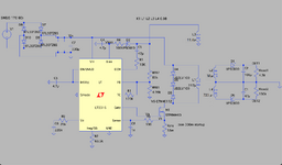
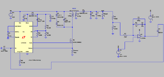
I designed a Multi-Winding/Multi-Output Flyback to generate +40V and -180V. In my application, the outputs need to work in a flip-flop load, where only one output handles a variable load of 0 to 50W at a time, while the other remains lightly loaded (just for stability). I used the LT8316 with no-opto (PSR) feedback, as shown in the attached file (some components are equivalent).

For the transformer, I used the TDK B66229G1000X187, with approximate inductances shown in the attached LTspice circuit. The winding specifications are:
  • Primary: 46 turns of AWG 22 (bottom layer)
  • Aux: 7 turns of AWG 28
  • Sec (+40V): 12 turns of AWG 22
  • Sec (-180V): 68 turns of AWG 22 (top layer)

I measured the leakage inductance at 13uH by shorting all the secondaries, including aux. This will make the K=0.98 (317/(317+6.5)).

Problem: In simulation with K=0.98, the outputs regulate well under any load. However, in the real circuit, the +40V rail drops to about +10V with even a 10W load, while the -180V rail performs well up to 45W.

In summary, the +40V rail has poor load regulation, while the -180V rail performs well. How this is possible and how to resolve? If the design is bad, how come -180v is performing well?

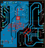
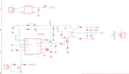
I've also attached my Schematic and PCB layout, which may not be ideal; however, even shortening paths (e.g., from aux to feedback resistor) has not improved performance.

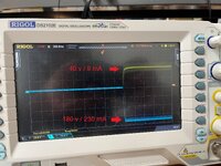
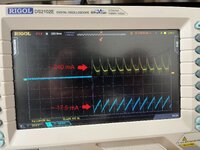
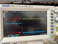
Also the OUT1 and OUT2 in different load levels have been attached.
 

Attachments

  • Screenshot 2024-10-20 at 3.44.55 PM.png
    Screenshot 2024-10-20 at 3.44.55 PM.png
    43.8 KB · Views: 48
  • Screenshot 2024-10-20 at 3.22.15 PM.png
    Screenshot 2024-10-20 at 3.22.15 PM.png
    83.6 KB · Views: 54
  • Screenshot 2024-10-20 at 3.14.40 PM.png
    Screenshot 2024-10-20 at 3.14.40 PM.png
    105.7 KB · Views: 58
  • IMG_6281.jpg
    IMG_6281.jpg
    1.8 MB · Views: 59
  • IMG_6280.jpg
    IMG_6280.jpg
    1.9 MB · Views: 43
  • IMG_6279.jpg
    IMG_6279.jpg
    1.9 MB · Views: 48
This is a classic newbie problem for newbies trying to design flybacks with more than one output and expecting both outputs to regulate even though only one ( or none in this case ) is actually controlled.

You can either; take feedback from both outputs and combine them for the control, or,

redesign the transformer so that the coupling between the 2 o/p's is really high, or,

both.

good luck @imijoon
 
Oscilloscope pictures suggest that the problem is mainly caused by instable operation in combination with asymmetrical filter capacitor sizing. This doesn't mean that transformer design is sufficient, but we need to see measurements with stable operation point.
As for inductance measurements, a complete Lij matrix should be obtained to determine coupling quality.
 
Hi,

I agree with easy_peasy.

Some members are annoyed when I explain that there are several issues with their design.
My posts are focussed on finding and solving the problem ... and never meant to personally annoy somebody.
So, if you can stand the truth ... ask for it.

In short: designing switching power applications is rather difficult. For every designer. Thus not recommended for newbies.
It needs understanding in GND_planes, HF principles, where are the loops of current and what is their impedance, high current, sensitive nodes... and so on.
As comparison: a switching power application is like a combustion engine .. with it´s explosions inside. You need to understand the forces of the explosions how to control them and how to use them.
The forces of the explosion are similar to the pulse currents of a flyback.

Klaus

added: Photos of scopes can be easily reduced to way below 100kBytes of file size without losing thread related informations. Tools usually are on your cell phone / camera, provided by each OS, and online for free.
 
And so...you dont actually need good coupling.
You say you need to regulate -180v, and then +40v, but never together.
So just bring on a feedback network...and use say an analog switch to switch from one of the outputs to the other, repeatedly as you require.
Beware of the "other" (non reg'd) output going overvoltage if its no-loaded, and the other output is on full load.....have a bit of dummy load say.
Very interesting suggestion. But this chip LT8316 meant to work as PSR (Primary Side Regulation). Can I still use in with an optocoupler (SSR) feedback as you suggested?
 
Yes you can reg it as attached in LTspice and PNG.
Similarly with an opto if you want isolation
 

Attachments

  • regd 8316.png
    regd 8316.png
    62.6 KB · Views: 27
  • 8316.zip
    1.8 KB · Views: 23
Before discussing about alternative regulation methods, we should at least try to understand why the original circuit is falling into hickup-mode with fully loaded 40 V output and possibly fix the issue.

According to datasheet there's no dedicated overload handling, just UVLO triggering if aux winding voltage and INTVCC collapses. Either this mechanism is causing instable operation or it's "only" the regular control loop. You should be able to determine by watching INTVCC.
 
Last edited:
Before discussing about alternative regulation methods, we should at least try to understand why the original circuit is falling into hickup-mode with fully loaded 40 V output and possibly fix the issue.

According to datasheet there's no dedicated overload handling, just UVLO triggering if aux winding voltage and INTVCC collapses. Either this mechanism is causing instable operation or it's "only" the regular control loop. You should be able to determine by watching INTVCC.

That's right, I'd like this to be resolved in the original config, as the intention behind selecting a PSR config was to simplify the design, and not be involved with opto-coupler feedback design. You are right, I didn't either see a mechanism for overload handling, but IREG/SS just for short circuit. I tried a big resistor on IREG/SS (equal to +200% of Inom) to avoid a false protection, but it didn't help. I will monitor INTVCC and see what I can see there.
 
Yes you can reg it as attached in LTspice and PNG.
Similarly with an opto if you want isolation
Curiously The LT1006 Op Amp has stable pulse oscillations at 4MHz indicating some deadtime with +fb (?) I had to choose diodes from my library with slight differences inside the P/N in order to Run it.

1730141476933.png


A few other unusual schematic settings with Rser of 20k on C9 only slow down the startup.

Time to change that OA.
 

LaTeX Commands Quick-Menu:

Similar threads

Part and Inventory Search

Welcome to EDABoard.com

Sponsor

Back
Top