Continue to Site

Welcome to EDAboard.com

Welcome to our site! EDAboard.com is an international Electronics Discussion Forum focused on EDA software, circuits, schematics, books, theory, papers, asic, pld, 8051, DSP, Network, RF, Analog Design, PCB, Service Manuals... and a whole lot more! To participate you need to register. Registration is free. Click here to register now.

Adding debug /test points in between the components in the RF front end design.

Maitry07

Full Member level 2
Full Member level 2
Joined
Jun 29, 2022
Messages
141
Helped
0
Reputation
0
Reaction score
0
Trophy points
16
Activity points
1,285
Hello,
I have designed one RF front end for my 4 channel receiver which include COTS components from recognized manufacturers such as Bias tee, LNA, attenuator, 4 way power splitter and band pass filters for 4 bands.
I have taken proper care for impedance matching in the layout. But still, I wanted to put test/debug points in between the components so that I can also check individual component's performance with spectrum analyzer. so, what is the best method in RF to put test/debug points so that this insertion cannot add any impedance mismatch and parasitic capacitance. what is the best practice to put this kind of test/debug points in the RF pcb through which any components can be accessed and tested via spectrum analyzer and it cannot affect the main signal path or performance of the overall RF front end chain?

request you to provide solutions for the same
 
You don't want "any" and some fancy dead guy said you can't make a measurement without perturbing the measured.

So get real and get quantitative.

Make two test articles. One for the assembly as you would deploy and one that is identical except for test access. Now you have a basis to quantity every test point's effect on lineup attributes and de-embed becomes practical.
 
Hi,

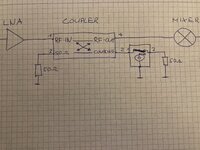
I very often use the connectors MM8030-2610 from Murata. With the proper cables you can measure the signals between the components with almost no influence. The connector opens the signal path. I had never problems with these connectors. If you don‘t want to open the signal path you can use a small directional coupler like the CP0603 from AVX in combination with the MM8030 and measure the signal. I use these methods many times. If you need the proper cable to connect the spectrum analyzer, I can send you the part number
 
With the proper cables you can measure the signals between the components with almost no influence.
I wonder how this can be.
At high frequencies every branch, every cable adds a new load to the test point, and each branch needs to be terminated properly, otherwise you get reflections.

Although I´m not very experienced in HF .. I´m with dick_freebird.
The best I can think of is an "almost identical" test unit, but with additional amplifiers to drive the test signals.

Klaus
 
Have a look at the dataheet of the connector. The connected cable opens the 50 Ohm transmission line with a cable 50 Ohm and the measurement device ( e.g. spectrum analyzer) 50 Ohm termination. Almost no reflections.
A second design is a good option, but to check power levels and component failures of 100 or more units you need debug points :)
 
Last edited:
yes, can you please send the part number. as well as can you share any of the reference scrrenshot of the schematic in which you have used MM8030-2610 AND CP0603 in between 2 components. so that I can take reference and guidance from that?
Actually, my RF front end is having more than 6 components interlinked with each other like LNA, attenuator, splitter, filter etc. and I wanted to check individual component insertion loss/gain with spectrum without its influence.
 
so, what is the best method in RF to put test/debug points so that this insertion cannot add any impedance mismatch and parasitic capacitance.
One easy method is to add a layout option where a 0 Ohm series resistor is placed one way (0°) or another (90° to the side), routing the signal into the next stage or routing it to a coax connector. My customers often use that method.
 
A Directional Coupler between two RF Blocks will replicate the Signal.
It might give you an insight at least how this block function.
 

Attachments

  • IMG_1493.jpeg
    IMG_1493.jpeg
    3.3 MB · Views: 29
Hi,

an example of how a photo can be reduced from 3406kBytes to 31kBytes ... (more than 99% of data omitted)
IMG_1493w.jpeg


Does it miss any thread related information?
 

LaTeX Commands Quick-Menu:

Part and Inventory Search

Welcome to EDABoard.com

Sponsor

Back
Top