Continue to Site

Welcome to EDAboard.com

Welcome to our site! EDAboard.com is an international Electronics Discussion Forum focused on EDA software, circuits, schematics, books, theory, papers, asic, pld, 8051, DSP, Network, RF, Analog Design, PCB, Service Manuals... and a whole lot more! To participate you need to register. Registration is free. Click here to register now.

LLC Resonant Converter

aneesh.r

Newbie
Newbie level 3
Joined
Jun 12, 2024
Messages
4
Helped
0
Reputation
0
Reaction score
0
Trophy points
1
Activity points
55
Hello,
I am trying to build a DC-DC Converter Circuit. The input is 50V, 10A. The required output at 1250V, 0.8A. The output power is 1000W. After multiple design iterations, I arrived at LLC Topology for the converter. An efficiency > 85% is required practically. Hence, LLC was the suitable option.

The converter is designed in the following stages:
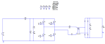
  1. Input Filter: An LC circuit with a 10uH Inductor and 120uF capacitor.
  2. Full Bridge Inverter: MOSFETs were operated with Phase Shifted gate pulses approach. AUIRFP4568 from Infineon were chosen as the MOSFETs which has Vdss = 150V.
  3. LLC Resonant Tank: The Resonant Capacitor was chosen to be 0.25uF. Film type capacitor was used for this purpose. The inductors were incorporated into the transformer.
  4. Transformer: A custom-made transformer was used. The leakage inductance between Prim-Sec, 10uH, played the role of the resonant inductor. The mutual inductance is 40uH. Turns Ratio is 1:6 (11 turns on Primary, 68 turns on Secondary).
  5. Full Bridge Rectifier: Diodes, C6D10170H, Silicon Carbide Schottky diodes were chosen. Vdc = 1700V
  6. Output Filter: Two 10uF capacitors connected in series is used.
The operating frequency is between 50-53kHz. The resonant frequency chosen is 51kHz. The load on the output side is a resistive load which needs to be varied between 750 ohms to 17500 ohms. The output required at different loads is different, the maximum being 1250V for 17500ohms.
The increase in phase shift, has to increase the output voltage, due to increase in power transfer cycle.
This circuit was rigged up and PCBs were fabricated for testing.
The following are the observations:
  1. The output at the full bridge inverter needs to be a switching waveform between -50V and +50V. But when the output was observed in the CRO, there were a few missing pulses (Image attached). What could be the reason behind this?
  2. Is the incorporation of the LLC Resonant tank inside the transformer a good approach?
  3. Since different outputs are required at different load values, is LLC an acceptable topology for this converter? This question is for the fact that in an LLC Topology the output is load dependent due to the reason that frequency changes with change in load.
  4. For lower load values, the output voltage trend was almost linear, with increase in phase shifts. For higher loads and higher phase shifts, the trend rose drastically. Is it regular in such converters?
  5. When an input of 50V is given, the gate waveforms experienced a lot of ringing. RC Snubber was introduced to the circuit to reduce the ringing, but there was no significant outcome from this. What is an alternative option?
  6. The MOSFETs in the full bridge are driven by UCC21521 gate driver IC which is placed external to the Primary PCB. Jumper wires were used for the interconnection. Is this a good approach?
The LTSpice Schematic of the DC-DC Converter circuit is attached for reference.
Can the above questions be answered?
 

Attachments

  • Full Bridge Output_Missing Waveforms.png
    Full Bridge Output_Missing Waveforms.png
    11.3 KB · Views: 130
  • LTSpice_Schematic.png
    LTSpice_Schematic.png
    46.7 KB · Views: 125
Sorry but you often say "phase shift"...do you mean the gate drives?...phase shifted operation?..as you know, in LLC, the drive is always 49% 49%..and the frequency changes.
 
Sorry but you often say "phase shift"...do you mean the gate drives?...phase shifted operation?..as you know, in LLC, the drive is always 49% 49%..and the frequency changes.
By phase shift, I mean that the operation of the Full Bridge is Phase Shifted Full Bridge Operation. The gate of the MOSFETs are driven by PWMs which are phase shifted. The duty cycle of the PWMs for the 4 gates are 50% with minimal dead time to achieve ZVS.
 
Sorry but you often say "phase shift"...do you mean the gate drives?...phase shifted operation?..as you know, in LLC, the drive is always 49% 49%..and the frequency changes.
1718256119906.png

QA and QB are switched at 50 % duty and180 degree out of phase with each other. Similarly, QC and QD are switched at 50 % duty and 180degree out of phase with each other. The PWM switching signals for leg QC – QD of the full bridge are phase shifted with respect to those for leg QA - QB. Amount of this phase shift decides the amount of overlap between diagonal switches, which in turn decides the amount of energy transferred.
 
You are apparently mixing LLC with PSFB (phase shifted full bridge) concept, I doubt that the approach serves the intended purpose. Besides unexpected load characteristic (4), you'll also get hard switching.

Regarding (5) and (6), I guess that jumper wires are causing gate voltage ringing, beside other possible layout issues.

Post #1 seems to suggest 1000 W output with 500 W input. I presume it's a typo.
 
What control chip are you using, or is it a micro?
I think LLC sounds best for you, as there is no overvoltage ringing in the output rectifiers.
Scrub the Phase shift full bridge. PSFB usually needs an output inductor, but i guess your leakage L is kind of doing that job.
There is something called a "Phase shift full bridge with resonant reset", which looks something like what you show.
But for you, the LLC, or the Series resonant converter looks good.
As of now the system is being operated in open loop mode. The control signals are given to the Gate Driver IC from an Atmega controller.
So is your suggestion to operate the circuit as a normal full bridge inverter and scrapping the Phase Shifted Concept?
Since LLC is the concept here, how can the change in frequency with respect to load phenomenon be addressed. Please provide some insights regarding this
 

LaTeX Commands Quick-Menu:

Similar threads

Part and Inventory Search

Welcome to EDABoard.com

Sponsor

Back
Top