goatmxj666
Member level 3

Hello RF PCB Experts
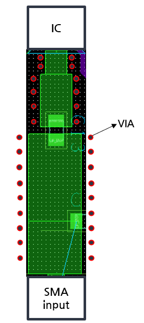
I have designed the input matching of an RF power amplifier with microstrip lines on a PCB as shown in the picture below. (The component in the middle is the capacitor footprint.)
My frequency is 2.4GHz.
I am designing a 3-layer PCB, the TOP layer is RF signal, the second layer is GND and the third layer is BOTTOM.
My question is, is it better to put a VIA around the RF signal line that goes through to GND as shown in the picture below, and if it is better to have a VIA, which one is better, "TOP-GND VIA" or TOP-BOTTOM through hole VIA?
It would be really helpful if you could let me know your experience.
