Continue to Site

Welcome to EDAboard.com

Welcome to our site! EDAboard.com is an international Electronics Discussion Forum focused on EDA software, circuits, schematics, books, theory, papers, asic, pld, 8051, DSP, Network, RF, Analog Design, PCB, Service Manuals... and a whole lot more! To participate you need to register. Registration is free. Click here to register now.

Solving adaptive frequency ..., process hf3d error: Failed to solve port 1, solving at too low frequency is a possible cause.

Ethan25

Junior Member level 3
Joined
Dec 17, 2023
Messages
29
Helped
0
Reputation
0
Reaction score
0
Trophy points
1
Activity points
254
Hi, I'm trying to simulate my NFC antenna in Ansys HFSS student 2023 R2 but Whenever I try to simulate it I'm getting the following error "Solving adaptive frequency ..., process hf3d error: Failed to solve port 1, solving at too low frequency is a possible cause. Please contact Ansys technical support. (04:25:38 PM Jan 10, 2024)" Ansys technical support is too slow and not user friendly that's why I have come here. thank you.

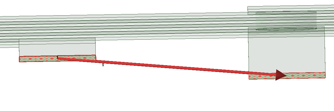
I'm trying to excite the port in a differential configuration like this. is this maybe causing the error ?
1704884821965.png
 
Alright, driven modal may not be the best to use given your setup. Are each of the red surfaces in your image individual ports? If so, this is incorrect. If not, can you please show your entire port setup?

Given your target frequency and geometry, I'd recommend switching to a driven terminal setup in either case.
 
The solution type should be HFSS and Options should be Network Analysis and Modal.


You may need a balun if you want differential E-fields, but this may be too low f for a small planar antenna with a large wavelength.

at 13.56 MHz What impedance? 100 ohms is near 1 uH 100 pF at 1nH/mm that's a big coil. you may want low Zo like 20 and high Q.

e.g. 1.5 cm square planar coil extremely sensitive to Dk of substrate. I'd do a 10% tolerance computation on Dk and tolerances on trace w,g,h to compute error sensitivity after you figure out the setup problem.


What are your design specs?

I'd go for 25 Ohm antenna to match ~ CMOS 74ALCxx driver 3 uH for a Q of 10 , higher to Q=50 may lead to tolerance issues but better sensitivity.

Are you going without ferrite pad? I would & get electrical testing for Dk, Zo ($)
 
Last edited:
Alright, driven modal may not be the best to use given your setup. Are each of the red surfaces in your image individual ports? If so, this is incorrect. If not, can you please show your entire port setup?

Given your target frequency and geometry, I'd recommend switching to a driven terminal setup in either case.
They are not individual ports.
I'm sorry but what do you mean by entire port setup ?
I have attached my .aedt file for your reference.
 

Attachments

  • Project5.rar
    30.7 KB · Views: 145
The solution type should be HFSS and Options should be Network Analysis and Modal.


You may need a balun if you want differential E-fields, but this may be too low f for a small planar antenna with a large wavelength.

at 13.56 MHz What impedance? 100 ohms is near 1 uH 100 pF at 1nH/mm that's a big coil. you may want low Zo like 20 and high Q.

e.g. 1.5 cm square planar coil extremely sensitive to Dk of substrate. I'd do a 10% tolerance computation on Dk and tolerances on trace w,g,h to compute error sensitivity after you figure out the setup problem.


What are your design specs?

I'd go for 25 Ohm antenna to match ~ CMOS 74ALCxx driver 3 uH for a Q of 10 , higher to Q=50 may lead to tolerance issues but better sensitivity.

Are you going without ferrite pad? I would & get electrical testing for Dk, Zo ($)
Yes, That is my solution type. "HFSS - Network analysis and modal"
my design specs are 40mmx30mm, track width and gap = 0.5mm and track thickness = 35um.

I have been trying to implement this in my HFSS project but so far I have not been very successful. I didn't change the impedance, it was in its default impedance of 50ohms.
 
They are not individual ports.
I'm sorry but what do you mean by entire port setup ?
I have attached my .aedt file for your reference.
Sorry, but I no longer have access to HFSS, you'll have to take some screenshots for me.
What exactly are you showing in your figure then? Please describe what you have done to set up your ports.
Here is what I would do:

- Ensure that the two conductors are seperate objects, i.e., they aren't united into a single object.
- Set your solution type to driven terminal. Tony seems pretty hung up on driven modal, but after ten years of nonstop simulations in HFSS my money is on driven terminal giving you a better result in this particular case.
- Create a rectuangular surface that insersects with both of the ends of your conductors, and extends somewhat around past the edges of both of them.
- Assign a wave port to this surface.
- Inside of the port settings, auto-assign terminals. Probably, you want one conductor to be the reference terminal.
- You should now be able to run the simulation.
- Feel free to try driven modal, in which case you can ignore assigning the terminals. It would make Tony's day, and I'd be interested to see how different the results are from each other.
Okay I tried both Modal and terminal.

Setup 1 : This is my first setup the red rectangle is what I have assigned as the excitation port. When I switch to terminal mode I'm getting the following errors : "Port '1': The number of terminals must be between 1 and 25" & "Port '1': The port has no terminals defined on it". In Modal mode wave port assignment I'm getting some result but it was not what I expected.

Setup 2 : I tried implementing vias in this like given in this. I initially tried to give excitation from one port to another port like in the previously mentioned forum post but whenever I do that I get the following error "Solving adaptive frequency process hf3d error failed to solve port 1 ...." I tried that with lumped port in driven modal method. To implement driven terminal solution I constructed a rectangle between the two feeds to like shown in setup 1 but whenever i did that I still got the same error of "Port '1': The number of terminals must be between 1 and 25" & "Port '1': The port has no terminals defined on it".
I can't tell what your Setup 2 figure is trying to indicate, but thanks for posting the images regardless.

I'm suggesting that you use a wave port -- not a lumped port -- with your driven terminal setup. The wave port is not a surface placed between the two lines, it is a surface that is normal to the the direction of the feedlines, that contacts the ends of the conductors. See several of the images here. When the wave port overlaps both conductors, you may assign terminals to it.
 
I
apart from errors, why does your design have such a small loop area?

Instead of this View attachment 187774
I was told more loop area in the middle will help have better read distance. and more over my design dimensions make it difficult to have such small packaging aswell
--- Updated ---

I can't tell what your Setup 2 figure is trying to indicate, but thanks for posting the images regardless.

I'm suggesting that you use a wave port -- not a lumped port -- with your driven terminal setup. The wave port is not a surface placed between the two lines, it is a surface that is normal to the the direction of the feedlines, that contacts the ends of the conductors. See several of the images here. When the wave port overlaps both conductors, you may assign terminals to it.
I was not able to use the wave port but I did continue with terminal setup as you suggested. I did check the difference between Terminal and modal but there was no significant change ?
can you tell me more about why you wanted me to go with terminal setup, I;m just curious. anyways thank you.
 
can you tell me more about why you wanted me to go with terminal setup, I;m just curious. anyways thank you.
Nothing terribly concrete, in the past I've just seen better performance with driven-terminal solutions at low frequencies and for this type of transmission-line setup. Ideally, driven modal and driven terminal would give the same results, so it's encouraging to see that that's the case for you.
If at all possible, I would try implimenting a wave port. It may solve your issue. There are many tutorials on youtube.
 
I

I was told more loop area in the middle will help have better read distance. and more over my design dimensions make it difficult to have such small packaging aswell
--- Updated ---


I was not able to use the wave port but I did continue with terminal setup as you suggested. I did check the difference between Terminal and modal but there was no significant change ?
can you tell me more about why you wanted me to go with terminal setup, I;m just curious. anyways thank you.
I don't know what constraints your size is but commercial ones are > 2 cm D

You were told right about the void area,
davg or average diameter is a better metric. (see formula)

Here almost filling the loop is only 50% more L than half as many turns with ~ 50% ID/OD
1705261328700.png

Of course one might use multiple layers to keep the mean D high, which raises cost and I only saw one edge of your design and no specs.
PCB costs tend to be the total area of initial Cu before etching of all layers in high volume regardless of nominal via count.
 
Last edited:

LaTeX Commands Quick-Menu:

Part and Inventory Search

Welcome to EDABoard.com

Sponsor

Back
Top