Continue to Site

Welcome to EDAboard.com

Welcome to our site! EDAboard.com is an international Electronics Discussion Forum focused on EDA software, circuits, schematics, books, theory, papers, asic, pld, 8051, DSP, Network, RF, Analog Design, PCB, Service Manuals... and a whole lot more! To participate you need to register. Registration is free. Click here to register now.

STA Primetime pessimistic hold timing check

Status
Not open for further replies.

titophe

Newbie level 4
Newbie level 4
Joined
Jan 7, 2010
Messages
7
Helped
0
Reputation
0
Reaction score
0
Trophy points
1,281
Location
France
Activity points
1,347
Hello,

I have a question relating to STA (Static Timing Analysis).
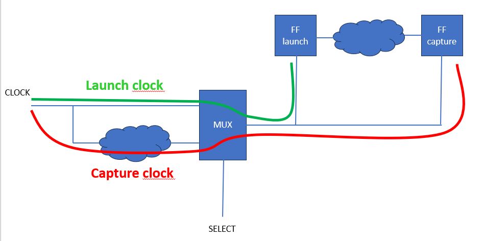
My design contains a MUX2:1 in its clock tree (cf. file attached).

I'm using Primetime from Synopsys for STA analysis.
In Primetime the timing report for hold check uses the "green" path for the launch clock and the "red" path for the capture clock.
To me this is pessimistic and unrealistic (As you know, for hold check, the same clock slope is used for launch and capture. In the real world the same clock slope can't go through the 2 input pins of the MUX at the same time and so the report is incorrectly pessimistic).

When I discuss this point with Synopsys, their answer is that it is a normal behaviour for an STA tool.

I'm wondering if someone could let me know if the other STA tools have the same behaviour (for example with Cadence Tempus).

Thanks in advance for your help
BR
cricri
clock_path.JPG
 

Solution
Thanks for your answer ThisIsNotSam.
You are totally right, there are different possibilities to workaround this problem.
On my side the workaround I use is to apply the command "set_clock_exclusivity -type mux -output <mux_instance_name/output_pin>. This works fine.

I had a discussion with Synopsys R&D on this topic. They are OK with my remark (physically speaking, 1 same clock edge can't go through the 2 inputs of the mux at the same time and so the report is unrealistically pessimistic).
I just want to know if the other STA tools behave the same for such clock scheme (for example Cadence Tempus).

Do you use Tempus or an STA engine from another EDA vendor?
What do you mean by clock slope? is it clock edge?
We use Synopsis STA tool for FPGAs.
The setup and hold checks are always from launch clock to latch clock but as follows:
setup: previous launch to current latch
hold: previous launch to previous latch
 

Yes I mean clock edge.

My question is about hold check. For hold check, the clock edge for launch and capture is the same (cf. attached snapshot).

Since this is the same clock edge which is used for launch clock and for capture clock, this clock edge can't go through one input pin of the mux for the launch clock and through the other input pin of the mux for the capture clock at a specific moment.

setup_hold_check.JPG
 

We agree on diagrams. Here is mine:

1694002959837.png

The idea is that the hold check makes sure that data arrival at D input of capture register is not too early as to violate the previous capture register timing window.
Similarly, the setup check makes sure that maximum data transition arriving at D input of capture register is not too late to violate timing window at current capture register.
 

Yes we agree on what are setup and hold checks.

I forgot to mention that the question is for an ASIC not for a FPGA.

As explained, the hold timing reports from PrimeTime is pessimistic and leads to insertion of unnecessary hold buffers in the datapath (which leads to performance loss and power consumption increase).

I'd like to understand if this pessimistic approach is the same for other ASIC STA tools or if they use a more realistic approach (for example Cadence Tempus).
The above check principles are fundamental and can't be tool dependent. In FPGAs we avoid gating clocks otherwise we also get hold failure and data path has to be delayed to offset the hold slack.
My guess is that you have a design problem but you think the tool is misbehaving. Let us hope somebody from ASIC community will help here.
 

OK thanks kaz1 for your answer.
I'm an ASIC designer and I'm not very familiar with FPGAs specificities. STA for FPGAs and ASIC is probably a bit different.

Is there an ASIC designer who is used to play with Cadence Tempus and who could check the behaviour of the tool when reporting an hold check for a design with such a clock path that contains a mux (cf. attached file to the first message of this thread)?

Thanks in advance
BR
 

If you have allowed both clocks to co-exist in your SDC, the tools is behaving properly. It must consider this strange case unless you tell the tool the clocks have no relationship to each other. see clock groups in your documentation. false paths can also fix the problem.
 

    titophe

    Points: 2
    Helpful Answer Positive Rating
Thanks for your answer ThisIsNotSam.
You are totally right, there are different possibilities to workaround this problem.
On my side the workaround I use is to apply the command "set_clock_exclusivity -type mux -output <mux_instance_name/output_pin>. This works fine.

I had a discussion with Synopsys R&D on this topic. They are OK with my remark (physically speaking, 1 same clock edge can't go through the 2 inputs of the mux at the same time and so the report is unrealistically pessimistic).
I just want to know if the other STA tools behave the same for such clock scheme (for example Cadence Tempus).

Do you use Tempus or an STA engine from another EDA vendor?
 

Solution
Let me ask one question: is your first diagram of register pair a specific part of RTL chain or is it just to demonstrate the whole RTL chain of a clock domain? in an RTL chain of a given clock domain, the same clock acts as launch and capture depending on chosen pair, ofcourse with some path delay.

If your diagram is a specific design pair that does not repeat across RTL you may have a way to de-constrain it. We need to see more detailed picture of such pair if so.
 

How does hold time required, compare to delay time? Is the
number sane? Have you made any effort to simulate what a
reasonable hold time minumum (incl negative) is (or is,
according to models and parasitics and fanout)?

"That's normal behavior" is not confidence-inspiring. Lots of
stupid is still "normal". Lazy and incomplete verification can
be "normal" too, when there's thousands of parameters to
check, at 4 per cell. Or whatever.

FFs are usually designed with zero hold time IME. Of course
you could find a way to screw that up if you were into the
transistor level design of the cell, but you aren't.
 

Thanks for your answer ThisIsNotSam.
You are totally right, there are different possibilities to workaround this problem.
On my side the workaround I use is to apply the command "set_clock_exclusivity -type mux -output <mux_instance_name/output_pin>. This works fine.

I had a discussion with Synopsys R&D on this topic. They are OK with my remark (physically speaking, 1 same clock edge can't go through the 2 inputs of the mux at the same time and so the report is unrealistically pessimistic).
I just want to know if the other STA tools behave the same for such clock scheme (for example Cadence Tempus).

Do you use Tempus or an STA engine from another EDA vendor?
Tempus. I haven't checked your scenario exactly, but I have a recollection of it working that way.
 

    titophe

    Points: 2
    Helpful Answer Positive Rating
Tempus. I haven't checked your scenario exactly, but I have a recollection of it working that way.

Hello ThisIsNotSam. Thanks for your answer.
If my understanding is correct, you have access to a Tempus license. Great.

I attached to this message a very simple gate-level verilog file and a primetime script.

The verilog file contains 2 D-FlipFlops that are clocked by the output of a mux. This mux2:1 has 1 input connected to the master clock and the other input connected to the delayed master clock.

Would that be possible on your side to update the verilog file with your standard-cells (replace the standard cells type surrounded by "###" ) and then source within Tempus a script equivalent to the primetime script attached. Sorry I don't know Tempus tool, its commands and its syntax but the script is very simple.

1/ read the standard-cells library
2/ read the verilog netlist
3/ link the netlist to the library
4/ create the master clock
5/ report hold timing in detailed mode in order to get the full expanded paths of the capture and launch clocks.

Note: do not set any value to the SELECT pin of the mux.

Thanks a lot in advance
 

Attachments

  • TESTCASE.zip
    787 bytes · Views: 116

Hello all.
Is there someone of you who could check this testcase using Tempus?
Unfortunately I just have a Primetime license but no Tempus License and my colleagues/friends are all using PrimeTime.
BR
Chris
 

Status
Not open for further replies.

Part and Inventory Search

Welcome to EDABoard.com

Sponsor

Back
Top