Continue to Site

Welcome to EDAboard.com

Welcome to our site! EDAboard.com is an international Electronics Discussion Forum focused on EDA software, circuits, schematics, books, theory, papers, asic, pld, 8051, DSP, Network, RF, Analog Design, PCB, Service Manuals... and a whole lot more! To participate you need to register. Registration is free. Click here to register now.

DC Biasing for Power Amplifier

Status
Not open for further replies.

hari_preetha

Full Member level 2
Full Member level 2
Joined
Jun 30, 2014
Messages
127
Helped
0
Reputation
0
Reaction score
0
Trophy points
1,296
Activity points
2,258
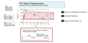
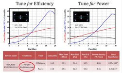
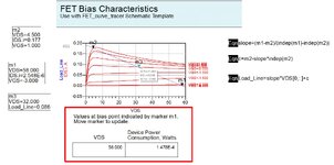
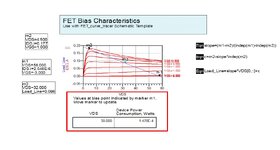
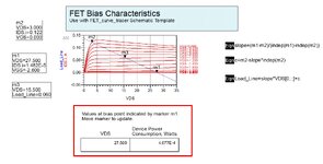
I want to design Ka- Band Power Amplifier using ADS software. I have taken 0.15 um GaN HEMT transistor for my design. According to datasheet, biasing conditions are VDS = 28 V and IDS = 100 mA. But when we checked DC IV Characteristics, I am getting operating point at VDS = 16 V, IDS =0.072 A, and VGS =-0.080 V in the active region. Once I select VDS =28 V, IDS =100 mA , am closer to Cutoff region.

I am getting confused by these two version, whether I have to follow datasheet biasing values or plotted DC IV characteristics values. Which I have to follow, clarify someone.
 

Attachments

  • DC_Load_Line_Analysis.jpg
    DC_Load_Line_Analysis.jpg
    269.2 KB · Views: 121
  • DC_Load_Line_Analysis_1.jpg
    DC_Load_Line_Analysis_1.jpg
    270.6 KB · Views: 116
  • Data_Sheet.jpg
    Data_Sheet.jpg
    142.9 KB · Views: 120

If your Vdd=28V, you should draw your Load Line from 2xVdd=56V (at least for Class-A)
Yes, I have varied VDS from 0 to 60 V. Then I am getting VDS=31 V, IDS= 0.088 A, VGS = -0.055 V in the active region. Then can I use these biasing VDS and IDS values for getting optimum output power, power added efficiency and gain. Please clarify it.
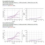
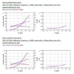
I'm not sure what that means, but the datasheet says 100mA/mm not 100mA.
Current in the right plot (Id vs. power) is not 100mA either.
As you mentioned 100 mA/mm, it is not 100 mA. As you mentioned 100 mA/mm, it is right only.
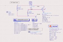
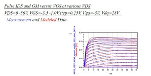
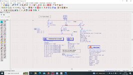
Below I have attached simulated DC-IV Characteristics and relevant datasheet screen shots. I am beginner to this PA design, please clarify my doubts regarding biasing.
 

Attachments

  • 29GHZ_Active_Load_Pull_of_ OSV_PA.jpg
    29GHZ_Active_Load_Pull_of_ OSV_PA.jpg
    218.2 KB · Views: 111
  • 29GHz_Load_Pull_Comparison.jpg
    29GHz_Load_Pull_Comparison.jpg
    74.6 KB · Views: 116
  • DC_IV_Characteristics_With_Load_Line.jpg
    DC_IV_Characteristics_With_Load_Line.jpg
    289.7 KB · Views: 112
  • Load_Pull_Measurement_at_Vd_28v_Id_100mA_mm.jpg
    Load_Pull_Measurement_at_Vd_28v_Id_100mA_mm.jpg
    123.3 KB · Views: 116
  • VDS_0_56V_VGG_-5V_VDQ_28V.jpg
    VDS_0_56V_VGG_-5V_VDQ_28V.jpg
    105.2 KB · Views: 117
  • Schematic_DC_IV_Characterstics.jpg
    Schematic_DC_IV_Characterstics.jpg
    454.7 KB · Views: 102
  • DC_IV_Characterstics.jpg
    DC_IV_Characterstics.jpg
    155.4 KB · Views: 113

Yes, I have varied VDS from 0 to 60 V. Then I am getting VDS=31 V, IDS= 0.088 A, VGS = -0.055 V in the active region. Then can I use these biasing VDS and IDS values for getting optimum output power, power added efficiency and gain. Please clarify it.

As you mentioned 100 mA/mm, it is not 100 mA. As you mentioned 100 mA/mm, it is right only.
Below I have attached simulated DC-IV Characteristics and relevant datasheet screen shots. I am beginner to this PA design, please clarify my doubts regarding biasing.
You cannot use this Operating Point for ALL purpose. There is no transistor in this world that will give these simultaneously. Load Line is just a starting point for getting an idea about Load resistance. The exact Impedance for ONE of the specifications above will be obtained by Load Pull + Source Pull simulations.
Let me give you a Hint. I have worked on this PA and found a valuable starting point.( Idsq=20.3mA)
The rest is yours. Yo can improve this amplifier to get better specs.
1693937030970.png
 
Last edited:
Let me give you a Hint. I have worked on this PA and found a valuable starting point.( Idsq=20.3mA)
The rest is yours. Yo can improve this amplifier to get better spec
Please let me know what about starting point of Vdsq. lt would help me lot.
 

Status
Not open for further replies.

Part and Inventory Search

Welcome to EDABoard.com

Sponsor

Back
Top