Smillsey
Member level 5

Hi all!
I am at the stage of manufacturing a pcb and in discussion witht he pcb fabricator regarding stackup (which they are trying to change, as usual!)
I have a 6 layer pcb, I have used layers as follows;
L1 : SIG
L2 : GND
L3 POWER PLANES
L4 SIG
L5 : GND
L6 : SIG
I set my stackup so that the spacing between 3 and 4 was much larger than the spacing between 4 and 5...
L3 -> L4 space was around 1mm
L4 -> L5 space was around 0.076mm
My theory was to "closely couple" the L4 -> L5, because L5 is a single solid ground plane and will be the return path for L4 high speed diff pairs and singled ended controlled impedance traces...
I wanted the L3 layer to have very limited affect on the impedance of L4, as it is not a single continuous plane....
I may be worried about nothing here, as L5 is a continuous plane and will provide the return path for the high speed signals, but can somebody put my mind at rest that I am okay to work as above? I am sure that as long as the "closely coupled" reference plan is continuous, this will be fine.... But any input would be appreciated
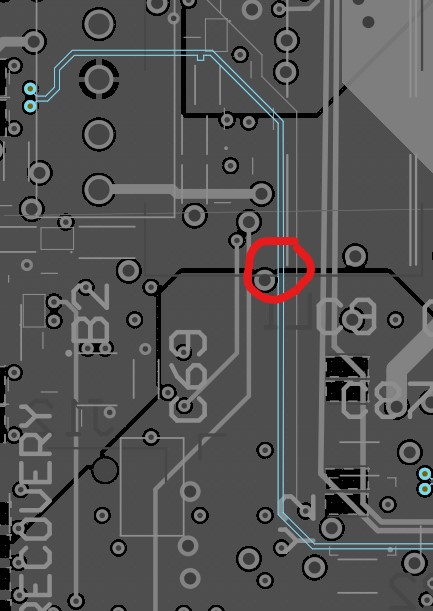
I have attached an example of what i mean.... You can see that the high speed trace passes over gaps in the power plane layer (which is 1mm away from the signal layer in question...) But i feel this will be fine as the ground plane for this trace is continuous and only 0.076mm from the signal traces and in my mind will provide a good return path.


