Continue to Site

Welcome to EDAboard.com

Welcome to our site! EDAboard.com is an international Electronics Discussion Forum focused on EDA software, circuits, schematics, books, theory, papers, asic, pld, 8051, DSP, Network, RF, Analog Design, PCB, Service Manuals... and a whole lot more! To participate you need to register. Registration is free. Click here to register now.

Low side mosfet switching and microcontroller sensing

Status
Not open for further replies.

vishweshgm

Member level 4
Member level 4
Joined
Dec 17, 2021
Messages
74
Helped
5
Reputation
10
Reaction score
7
Trophy points
8
Activity points
952
Hello,

I am designing a battery discharger that can discharge upto 200A on 100V. I want to allow user to configure discharge current configurable using pushbutton and LCD.
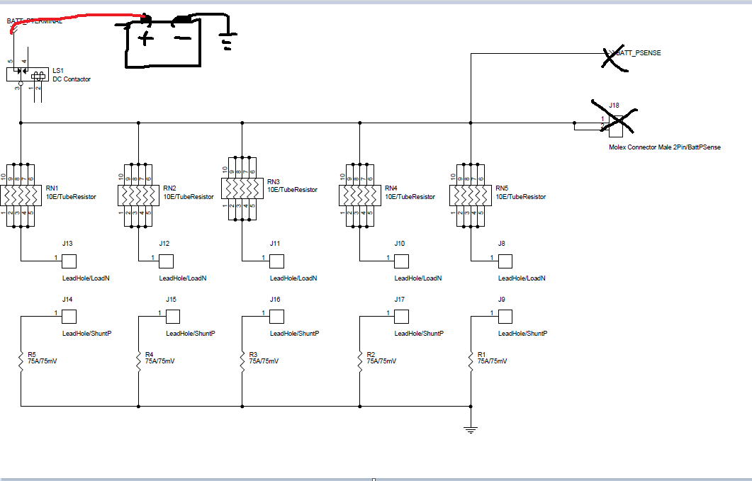
Here is my plan:
1670403842335.png


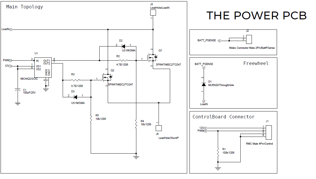
I plan to use tube resistors of 1200W,10ohm each in parallel so that for 100V it is capable to dissipate upto 250A. To control current A, I plan to use simple low side switching mosfet. I used a 5 PCB boards equipped with 2x 47A paralleled mosfets (total 5x2 = 10mosfets AND 5 driver chips MIC4422), so that for 200A, each mosfet will have 20A each, or 40A on each power PCB.

Power PCB schematic is as shown below. such PCBs and pwms are used. PWMs are given from another controller board that I have not shown.
1670403914313.png


Now my questions:
1. I set-up everything and given pwm from controller and all of a sudden controller board resets.
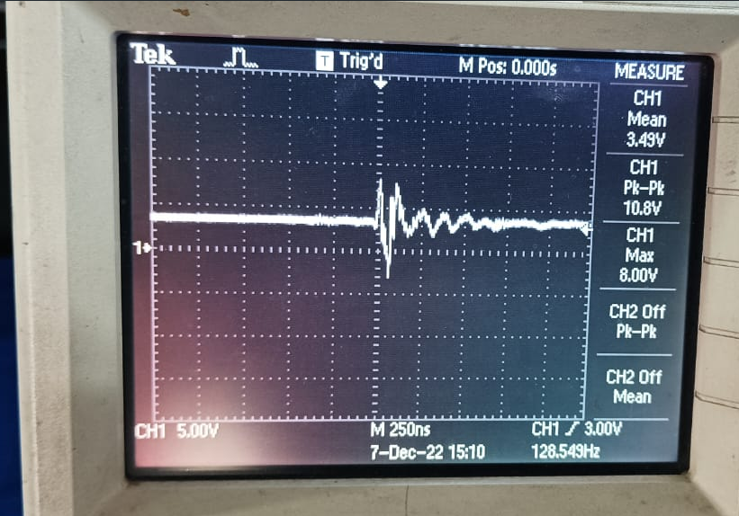
A close examination reveals that, on 3.3V supply (microcontroller supply), I am seeing a noise like this. This is happenign at mosfet switching off moment.
8V Max that you see is when only one mosfet board is being switched on, but it shoots upto 40V when multiple pwms on pcbs are turned on (which is my normal usecase). At this time controlller resets.

Here is the strage part, controller board grround (-ve of supply ) and battery-mosfet path ground is isolated using PC817 opto-coupler.
1670404846138.png


I am going crazy as this was absolutely not expected. when PWM is is isolated from controller supply, why does the controller supply pickup noise only when switching is running. Note that if I make pwm to be 0 or 100% there is no noise and controller runs properly. I elimineted issue in controller pcb by removing battery and running the switching pwm. This time there is no noise.
Also, my pwm frequency is only 50Hz, as I donot need mosfets to be switched fast for this application.

2. My second question is there any other easy low-cost way to achieve what I want? I am aware of using IGBT, yet it too has switching circuit which might result in same problem.
 

Hi,

My first question:
Do you really want to "waste" up to 20kW of heat? Where do you expect the heat to go to?
(I mean: My whole house does not need that much heat in winter)
I´d consider to use this energy. Maybe using an inverter to push it back into the grid. This way you don´t need the huge effort to get rid of the heat, while at the same time you get money.

Other questions:
Why all 5 of them PWM´d? You can do the same with 4 ON/OFF and only one PWM.

What is the goal of this?
What (electrical) value you are interested in?
What resolution and accuracy do you need?

*****
Solutions could be
* simple ON/OFF switching various loads
* no current measurement at all
* or current measurement through one commmon current transducer

*****

The "spike" problem:
* maybe is by ground bounce due to high currents, fast switching, unsuitable wiring
* maybe is caused by the inductance of the tube resistors
* or something else
hard to say .. because we don´t see your application, especially GND wiring, maybe there even are ground loops.

Your driver circuit uses one single GND for logic_reference as well as for MOSFET_reference. This calls for GND loops.
There are drivers that have pins for logic_gnd and MOSFET_reference (or however you may call it).
You may also use galvanic isoation maybe using optocouplers.
(Usually I tend to use clean wiring instead of isolation, but in your case the isolation may be a rugged and suitable solution)


Klaus
 
These folks make modules, single parts, into the 1000A+ area.


And these folks into your range (single parts) :


Regards, Dana.
--- Updated ---

The spike quite likely stray L, and at these current levels produces significant
V spike when switch opens. Also keep in mind the MOSFET body diode in this
part, whicg turns on in sw off transient, is not a fast diode, so peak V's will be
higher than if a fast or ultra fast diode is added in parallel to body diode.

Here is a representative comparison with a Schottky diode versus the intrinsic body diode :

1670423153099.png


Regards, Dana.
--- Updated ---

Note the curves two different process MOSFETs, no external diode, but
a much faster body diode in the enhanced MOSFET.

So either pick a faster MOSFET with a fast body diode or use one external.
And pay careful attention to parasitic L, it is at these current levels a
monster under the bed. The inverter and welding guys know a lot about
these design issues.


Regards, Dana.
 
Last edited:
I don't see how transistor body diodes can be reverse biased in this application. Respectively there's no reverse recovery.

I can well imagine that large transients can be produced with inappropriate control circuit connection. Unfortunately the design details are unclear, how is optical isolation used, how is the power supply connected, where is the waveform probed?

There's no need to switch multiple load modules at a time.

My post # 3 is in error, as FVM points out. The turn off of the MOSFET results in a rise of
drain V until breakdown occurs. A clamping effect. The tolerance of the MOSFET to this
breakdown is complicated by type of MOSFET, LV vs HV, and its design/architecture/technology.
Avalanche can also result.

So to FVM's point, there are no reverse recovery considerations for body diode in this general design.

That being said doing a sim one can see a small fwd bias on body diode, but if models are
correct (I looked at several) its << 1V so essentially not a design consideration.


Regards, Dana,.
 

Hi
Thanks everyone for suggestions. Here are my updates. Today partial solution is found.

1. The culprit was D2 and D3 gate diodes. While testing I removed these and suddenly the noise on 3.3V line shown in my image in #1 is gone and controller no longer resets and works fine. I have no idea why this got solved due to diodes theoretically.

2. Further, another crazy thing was gate resistors if changed to 680ohm, gives a more beautiful,neat Vds waveform instead of 4.7ohm.

3.Now that, I solved this issue working with one powerPCB (i.e able to handle 40A max) separately, it is time to run all 5 power pcbs connected together with load as shown my diagram in post #1.

4. I connected everything and gave 10% duty cycle, 50Hz, to all 5 power pcbs at the same time. Suddenly 2 mosfets in one of the PCBS got FRIED HORRIBLY. Here I stopped today. Progress is that even though PCB fried my micrcontroller board running just fine. Note that I had individually checked for 10% duty cycle, by turning pwm on each one of the pcbs individually (battery voltage 110V) before turning all of them at once.

5. Many pointed out that voltage spike could be high during turn off and I'll try snubber suggestion by @Easy peasy tomorrow.

6. Also circuit seems unclear to you here I explain again:
I designed this circuit to be able to configure to have either isolated ground or common ground.

Referring circuit below, GND1 and GND2 are always common.

I can make GND3 either isolated or common (Ignore sensing for now). I have given powerpcb schematic in #1
1670517583322.png


Right now, All 3 GNDs are common in my circuit.

Do you really want to "waste" up to 20kW of heat? Where do you expect the heat to go to?
(I mean: My whole house does not need that much heat in winter)
I´d consider to use this energy. Maybe using an inverter to push it back into the grid. This way you don´t need the huge effort to get rid of the heat, while at the same time you get money.
Unfortunately we have to waste. The application used in re-generating the old batteries (gel type) where they have to charge discharge mutiple times. We cannot provide inverters as these instruments need to be carried around to various places and service needs to be provided. If any corporate management has "real concern" they might invest to have this energy re-use infrastructur at their site.
What (electrical) value you are interested in?
Max volt 110V, Current configurable upto 200A
What resolution and accuracy do you need?
need not be very accurate, should within 2-3Amps bandwdith of configured current. I can also say minimum 50A must be drawn not less than that.
Solutions could be
* simple ON/OFF switching various loads
Simple on/off doesnot help me as I want to design a constant current discharging. If I design simple turn ON/OFF design, discharge current decreases as voltage drops
hard to say .. because we don´t see your application, especially GND wiring, maybe there even are ground loops.
I have given a ground connection details.
Unfortunately the design details are unclear, how is optical isolation used, how is the power supply connected, where is the waveform probed?
I hope my diagram gives clear details. each pwm was isolated using pc817 using circuit like this below. Crazy thing is even with this isolation, i was getting noise on 3.3V,GND3 line.
Probe was connected between 3.3V and GND3.
1670519003445.png


Anyway, after removing D2& D3, this noise is gone. Wwithout isolation it works fine. So right now I removed all isolation and GND1,GND2, GND3 are common.

There's no need to switch multiple load modules at a time.
Sorry, I donot understand. What topology do you suggest? I donot want to go for single mosfet designs using SiCarbide mosfets as it becomes too costly.
Also you are turning your mosfets on too fast - try 47 ohm ....
Your suggestion seems right, but not 47ohm, 680ohm made waveform more neat.
 

Attachments

  • 1670518821970.png
    1670518821970.png
    63.5 KB · Views: 139

Your change to 680 ohms in the gate I think big part of your problem. Here is turn on
transient, as you can see MOSFET spending way too much time in active region, hence
dissipating a lot of power.

Note I could not find C2 spice model, so using C3. Also note not sure why the sim is
showing a static Pdiss of 180W when fully on, maybe the C3 Rdson much higher than C2 ?

1670523385642.png


Normally one uses Rgate to eliminate parasitic L effects causing oscillation. Runs in range
20 - 100 ohms.

Some help determining :


Can you post a scope single shot event of Vgs and Vds during turn on, for both 680 and say
20 ohms ?


Regards, Dana.
 
Last edited:
If you take up the suggestion to throw load power to a
useful purpose rather than waste heat, check out
"regenerative load" as a subset of electronic loads.
Basically you use a current mode controlled PWM
to force a sink current, "losslessly".

What use you'd put it to... maybe charge the other
batteries waiting for load test?
 

Simple on/off doesnot help me as I want to design a constant current discharging. If I design simple turn ON/OFF design, discharge current decreases as voltage drops
You missed my words "various loads". 7 switches could give 128 steps of 2A each. Really constant current.

But using PWM does not give constant current.

Klaus
 

showing a static Pdiss of 180W when fully on, maybe the C3 Rdson much higher than C2
Post#1 says 20A per transistor, not 50A.

Switching losses with 680 ohms gate resistor are high, but well within SOA. The achieved switching speed is in the ballpark for low frequency, low EMI application.
 

47 ohm - 82 ohm will be optimum - 680 ohm will fry your fets due to peak switching losses and lack of liquid N2 to cool fets.
 

Post#1 says 20A per transistor, not 50A.

Switching losses with 680 ohms gate resistor are high, but well within SOA. The achieved switching speed is in the ballpark for low frequency, low EMI application.

Post # 9 shows 2 ohm loads.....and OP talks about 40A......

We also do not know if at 680 ohms his gate in prolonged oscillation that
sim is not picking up. Sim does show hi static Pdiss, Rdson calc would have that
at 112W @ 40A, sim shows 180W....not sure why w/o investigating model. But my
sim shows Id ~ 55A, so maybe thats key to the high static Pdiss. And we do
not know his thermals.

SOA he is right at the limit with Vds ~ 3V, Id 40A, 20 mS. No margin. And he is getting failures.

Hopefully he can post pics of prototype, and maybe some scope shots.


Regards, Dana.
 

your SOA calc's possibly do not include the inductive energy of the load at turn off - especially for solenoid wound resistors.
--- Updated ---

peak dissipation at 110VDC and 10A is 275 watts during the crossover at turn on or off

for 40A it is 1100 W

in either case due to inductance of resistor the V will rise to the clamping level of the fet ~ 650V ( initially at full current ) - until the time constant of the R & L are exhausted.

this is 6500 W briefly for the 10A case, and 26,000 W briefly for the 40A case

So carefully choosing R-on and R-off are important, as is reducing wiring inductance, load inductance and having good snubbers across the fets.
 
Last edited:
Here is turn on comparing 50 and 680 ohms in gate, 100 nh assumed stray L :

1670550356339.png


Regards, Dana
 

I agree about load inductance problem. Seriously noone would operate the switch without freewheeling diodes.
--- Updated ---

Partial correction, If toff is larger than the inductive time constant RL*Lstray, there's no inductive overvoltage. If the circuit layout doesn't allow freewheeling diodes that span the complete load circuit, you'll either go for slow switching (sufficient high gate resistors) or implement active clamping, zener diodes that turn the MOSFET on before it goes into avalanche breakdown.
 
Last edited:

Status
Not open for further replies.

Part and Inventory Search

Welcome to EDABoard.com

Sponsor

Back
Top