Continue to Site

Welcome to EDAboard.com

Welcome to our site! EDAboard.com is an international Electronics Discussion Forum focused on EDA software, circuits, schematics, books, theory, papers, asic, pld, 8051, DSP, Network, RF, Analog Design, PCB, Service Manuals... and a whole lot more! To participate you need to register. Registration is free. Click here to register now.

MSTEP component

Status
Not open for further replies.

mohamis288

Full Member level 3
Full Member level 3
Joined
Mar 1, 2022
Messages
165
Helped
0
Reputation
0
Reaction score
1
Trophy points
18
Activity points
1,234
Hi,
I know that MSTEP is necessary for simulation parasitic discontinuity. For example, discontinuity between two T.L. with different length. But recently, I find out we can use that as discontinuity for component lead. There is a document from NXP about that but I can not understand it. I mean it differs from what I understand in the previous application. For example, there is discontinuity between the component lead and lead pad. Also, there is discontinuity between lead pad and transmission line which is connected to it. So I should use two MSTEP component. no need to mention that MSTEP Does not add any trace in layout. Can someone explain it?
 

Attachments

  • EB212.pdf
    167 KB · Views: 295

MSTEP models the effect of a change in width. At every step, the current wants to stay on the edge, and re-distributes to the new line width. That causes inductance and possibly shunt capacitance to ground, and element MSTEP models these parasitics.

Another use of MSTEP is when a transistor lead is smaller than the copper it connects to. Same situation: the current must re-distribute, and we use MSTEP to model that.

I created the picture below using EM simulation to show current density at such changes in line width. When using circuit models, MSTEP is used to represent these discontinuities.
step.PNG
 
Review MSTEP paragraph in ADS manual. It's explicitely dedicated to model the effects of the transition between microstrip TL of different widths. Chaining MSTEP elements without a TL of relevant length in between is beyond the specified purpose and unlikely to improve circuit modelling.

Footprint pads should be included in the component model in case of doubt. Clarify how the component model is defined, what's the reference plane and expected wiring.
--- Updated ---

If we have relevant connecting transmission line segments as in the example shown by Volker, MSTEP can be of course used.
 
RF power transistors usually have leads that connect to much wider copper lines, and that is a perfectly valid use case for MSTEP, as described in the appnote. That physical step in width from line to device is modelled properly using MSTEP. There is no component "pad" in this case.

(I have worked on a few customer cases where the step in width was no properly modelled at this transistor connection: big issue! This is a low impedance point and the step in width has a massive effect.)

step_mgf0907.png
 
Last edited:
MSTEP models the effect of a change in width. At every step, the current wants to stay on the edge, and re-distributes to the new line width. That causes inductance and possibly shunt capacitance to ground, and element MSTEP models these parasitics.

Another use of MSTEP is when a transistor lead is smaller than the copper it connects to. Same situation: the current must re-distribute, and we use MSTEP to model that.

I created the picture below using EM simulation to show current density at such changes in line width. When using circuit models, MSTEP is used to represent these discontinuities.
View attachment 175124

RF power transistors usually have leads that connect to much wider copper lines, and that is a perfectly valid use case for MSTEP, as described in the appnote. That physical step in width from line to device is modelled properly using MSTEP. There is no component "pad" in this case.

(I have worked on a few customer cases where the step in width was no properly modelled at this transistor connection: big issue! This is a low impedance point and the step in width has a massive effect.)

View attachment 175126
thank you for your answer. well,I Have read the tutorial about MSTEP in keysight website. but medeling is my main problem. I think it is better to clarify my question.
imagine that I want to connect a SMD resistor with lead width equal to 5mm to a lead pad with width and length equal to 7mm and 3mm respectively. this lead pad is followed by a transmission line with width equal to 6mm. so, what I think to do is present in the attachment. is it correct?

manual schematic.jpeg
 
Last edited:

You are mixing width and length, w3 is the pad length !?

The situation that you have drawn in your last picture would modeled like this:

MLIN w=6mm l=??mm
MSTEP w1=6mm w2=7mm
MLIN w=7mm l=3mm

... but here are my comments:
a) You don't know what is the reference plane of the component. If we include the 3mm pad length using MLIN, the SMD reference plane must be at the inner side of the pad. Often SMD data is specified with reference plane at the outer side of the pad, then we would include too much length (too much phase) if we add MLIN of 3mm length for the pad. There is no simple, universal answer to this, it depends on your SMD data and how they are measured/specified.

b) The effect of a step in width from 6mm to 7mm is small, so here the MSTEP is not so very important.
Hi again,
sorry for taking your valuable time Volker. I hope to compensate your kindness.
I had attached another picture but I don't know why, this was deleted.( that was from the ADS environment, maybe I should crop it. maybe it was deleted because of copyright.) I attach it again to this response. so to explain more:

You are mixing width and length, w3 is the pad length !?
yes, I have used W3 instead of length.

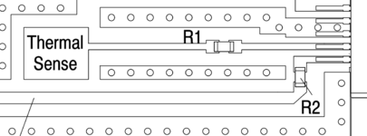
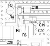
a) the length and width of the pad are chosen arbitrarily. no need to pay attention at the values. in fact part of the board that I want to make at first is here in the attachment. consider R1 in "part of simulation" picture. ( SORRY! I do not know what do you mean by the INNER and OUTER side of the pad.) as you can see, neither leads in R1 are connected to reference plane. but in "part of simulation 2" picture, you can see that C19 and C20 are connected to reference plane. but modeling R1 is desired here.

if it is possible, please attach a picture of the schematic in software environment like below.
 

Attachments

  • software schematic (3).png
    software schematic (3).png
    19.8 KB · Views: 163
  • part of simulation.png
    part of simulation.png
    47.2 KB · Views: 134
  • part of simulation 2.png
    part of simulation 2.png
    70.5 KB · Views: 135

You misunderstand some words.

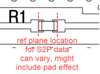
The word "reference plane" does not mean ground. Reference plane means the plane (location) where the phase reference for S-parameters is. Talking about components, it makes a difference if the S-parameter phase reference is at the begining (outer side) or the end of the pad (innder side). I hope you now understand what I mean.

This is an important concept is using S-parameters for SMD devices, because depending on the S2P data ref plane the pad effect might be included (fully or partially). We don't want to ignore pad effect, but we also don't want ito include it twice if it is already included in the S2P data.

For your ADS model with R_PAD the idea looks ok, but you have swapped W1 and W2.
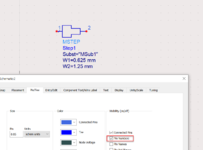
For correct use of W1 and W2 at the MSTEP, you can switch on node number display in Options > Preferences, so that you know which side of the STEP is W1 and W2.
 

Attachments

  • refplane.png
    refplane.png
    25.4 KB · Views: 130
  • pinnumber.png
    pinnumber.png
    37.5 KB · Views: 146
Last edited:

Status
Not open for further replies.

Part and Inventory Search

Welcome to EDABoard.com

Sponsor

Back
Top