Continue to Site

Welcome to EDAboard.com

Welcome to our site! EDAboard.com is an international Electronics Discussion Forum focused on EDA software, circuits, schematics, books, theory, papers, asic, pld, 8051, DSP, Network, RF, Analog Design, PCB, Service Manuals... and a whole lot more! To participate you need to register. Registration is free. Click here to register now.

4017 driver schematic

Status
Not open for further replies.

sheldonstv

Junior Member level 2
Joined
Aug 16, 2006
Messages
21
Helped
1
Reputation
2
Reaction score
1
Trophy points
1,283
Location
UK
Activity points
1,391
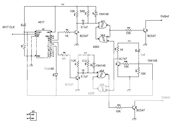
4017latch.jpg


simple schematic..........
 

what circuit it is? what is the timing diagram of two o/p line?
 

It seems to be a DC to AC converter...
 

It has the same function as this one.


But the auther has improve to use the microcontroller as this one.
 

4017latch.jpg


simple schematic..........
ok,i agree with you,its a very simple circuit .....but its us......................................................
- - - Updated - - -

4017latch.jpg


simple schematic..........
OK,I AGREE WITH YOU,ITS A VERY SIMPLE CIRCUIT .....BUT ITS USE......................................................
 

The title in the link I given said that "Modified sine wave inverter".
 

sine wave ?noooooo i uploaded the wrong image..... heres the correct file
 

Attachments

  • FLASHCHASECAD.2.pdf
    10 KB · Views: 150
Last edited:

Status
Not open for further replies.

Similar threads

Part and Inventory Search

Welcome to EDABoard.com

Sponsor

Back
Top