OZZAA
Member level 1

I tried to start designing a Class C power amplifier at 5 GHz (for any vlaues of gain and output power)
I used TSMC 180 nm technology.
I build the following circuit to test some concepts

I found that the max available gain is in -dB (Attenuator)
also when I modified the terminals' impedances as shown in the circuit the S21 is also -dB (attenuator)

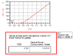
the gate bias voltage is 0.1< (Vt=0.5 V) as shown in the following figure

What is the problem
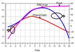
If the gain is still -ve the PAE will go to -ve values, is not it?
Any Help will be highly appreciated
I used TSMC 180 nm technology.
I build the following circuit to test some concepts

I found that the max available gain is in -dB (Attenuator)
also when I modified the terminals' impedances as shown in the circuit the S21 is also -dB (attenuator)

the gate bias voltage is 0.1< (Vt=0.5 V) as shown in the following figure

What is the problem
If the gain is still -ve the PAE will go to -ve values, is not it?
Any Help will be highly appreciated


