Continue to Site

Welcome to EDAboard.com

Welcome to our site! EDAboard.com is an international Electronics Discussion Forum focused on EDA software, circuits, schematics, books, theory, papers, asic, pld, 8051, DSP, Network, RF, Analog Design, PCB, Service Manuals... and a whole lot more! To participate you need to register. Registration is free. Click here to register now.

[SOLVED] uc3842/3843 Vcc problem in smps.

Status
Not open for further replies.

codemaster11

Advanced Member level 4
Full Member level 1
Joined
Sep 2, 2019
Messages
115
Helped
9
Reputation
18
Reaction score
7
Trophy points
18
Activity points
1,221
i 'm facing the problem of uc3843/3842 VCC in a uc3843 based smps that show Vcc about 86vdc or even greater

when the power mosfet & ic is not in the circuit. but when i place the ic, the voltage through kick resistor drop to 6.5v. the kick resistance value is 150k/2w.

i blow up three 13n50 mosfets today because of this problem. the smps blow the mosfet in seconds. i have another circuit that works correctly and show

Vcc = 17vdc arround not greater when the mosfet & the ic is not in the circuit, with the same kick resistance, placing mosfet & ic.

Vcc drop to about 12v and the circuit works correctly. both circuits have same pcb layout but i don't know why this high voltage appear at the Vcc of ic ???

the value of kick resistor is the same as before.
 

I think you should use an R/ZENER/BJT startup regulator...(high voltage BJT)

Diode OR it out when the bias winding gets up to voltage

(also, are you sure its UC3843 and not the lower current taking UCC38C43?)
 
you need to post the schematic - you are doing something wrong - but the magic crystal ball is clouded over by lack of real information ...
 
  • Like
Reactions: treez

    T

    Points: 2
    Helpful Answer Positive Rating
i 'm using uc3842/uc3843, i made the smps many times and its works fine this problem doesn't arise

in working power supply, but sometimes this problem occurred with me but i dont know its reason why this high voltage comes at Vcc.

i check it with DMM there is no direct connection with Vcc from main bulk capacitor. i don't have the schematic but this is the PCB layout.

the symptoms of this problem is that for the first time the smps start normally and when i put load on it

the power mosfet blow that also damage the ic the current sense 0.22R/2w resistor and 1.5k resistor from pin # 3(Isense) of the ic connected with current sense.

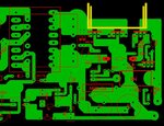
after that i replace the components but still the Vcc showing above 80vdc. but i 'm stuck in finding the reason of the fault? below is the PCB layout.

capture1.JPG

capture2.JPG
 

Hi,

, i made the smps many times and its works fine
i don't have the schematic
How can you "make" this smps without having a schematic?
Did you even read the IC's datasheet and application notes?

PCB without GND plane, and a PCB layout that seems not to comply with common safety standards.

In my eyes you risk health of the users of this supply. Thus I leave this thread.
Take care.

Klaus
 

Sorry but none of the documentation provided helps to solve your issue - schematic please - it could be that you are running off an isolated transformer and then the gnd of the scope probe is earthing one side of the power ckt and causing issues that way - without detailed photo's of the actual setup and schematics no one can help you ...

- - - Updated - - -

you haven't got safety separation under the opto - also the tracks to your main fet are waaaaaaaaaaayyyy too long ...

- - - Updated - - -

your 150k 2W resistor to the IC needs a zener to gnd, else you will overvoltage the IC ...
 

this is not the final layout with all possible safety protections. i currently working on this power supply testing for my own purpose.

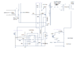
the final layout will be redesign by expert pcb designer, that's not the problem. i made a rough schematic according to my layout as i studied many

uc3843 smps circuit on the web and made it.

this is the schematic below.
Untitled.png
 

Hi,

this is not the final layout with all possible safety protections. i currently working on this power supply testing for my own purpose.

the final layout will be redesign by expert pcb designer, that's not the problem. i made a rough schematic according to my layout as i studied many
Nobody wold build a house on weak surface with unsuitable material to test it's quality. Then build the real house with completely different conditions.
My recommendation: Do the tests on a circuit PCB layout that most perfecty fits the final state.
Otherwise you risk that
* you spend much time on PCB layout problems that never would exist on the final PCB layout...or
* you make the "test version" running by accident, but the final version refuses to work (reliably).

Klaus
 

off course there is no zener on the Vcc to limit voltage. but i'm not sure whether it will solve the problem or not.

if i place the zener on Vcc will it stop blowing the power fet?
 

Simple logic tells you that if the IC fails through over-voltage it is likely that over-voltage will make it to the gate pin, holding the fet on, and/or destroying the gate structure, again turning the fet on - and then bang ...
 
dear i tested this circuit by building it in my home at least about 5 times. also i didn't place the zener on the Vcc it works fine for hours

i tested it with 12vdc/80 watt car headlight. the voltage also not going above Vcc = 18vdc, i tested it upto 230 watt output. it works without any

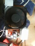
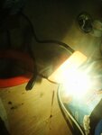
problem. i don't have the complete image of the design. but i can show a picture with 80 watt/12vdc light at its output.

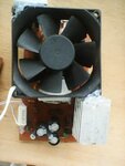
Photo0409.jpg Photo0410.jpg Photo0419.jpg

this circuit is tested upto 230watt output power & works for hours & still it is in working, it also don't have zener at Vcc.

- - - Updated - - -

but now this problem arise when the fet blow first time in a newely design circuit & also expectedly this high voltage at the Vcc cause this problem.
 

the problem here is lack of cognitive function, without a zener the Vcc will be exceeded if the IC does not start ....
 
i think this might be the problem & there is no difference b/w the working and not working circuit. then how to solve this problem ?

- - - Updated - - -

Simple logic tells you that if the IC fails through over-voltage it is likely that over-voltage will make it to the gate pin, holding the fet on, and/or destroying the gate structure, again turning the fet on - and then bang ...

how the problem pointed can be avoided ?
 

there is no limit on the duty cycle if the feedback, via opto, does no work properly. There is a 36V zener inside the chip on the Vcc line - but this is low power ...

if the feedback isn't wired properly or the opto is dead - then the pwm will go up too high & bang ...
 

Hi,

dear i tested this circuit by building it in my home at least about 5 times. also i didn't place the zener on the Vcc it works fine for hours i tested it with 12vdc/80 watt car headlight. the voltage also not going above Vcc = 18vdc, i tested it upto 230 watt output. it works without any problem
Ask yourself:
* It works (by accident), just because you observed it's final function for some hours...
* or it works reliably, because you kept on specification and design rules

I refuse to take care of traffic while passing a crossing. It works for days now. It's proven.
Does this concept reliably work for the future?
It's your decision how you do your designs...but don't be surprised if it does not work..

Again: Don't risk your or other's lifes. Not only by electrical shock. Not caring abot specifications also may cause overheat and fire.

Klaus
 

i tell one's before this i didn't sell in the market not intend to sell it. i'm currently working on it. also you only criticizing not telling about the problem sorry

please leave this thread & don't waste time.
 

Hi,

One last comment.
also you only criticizing not telling about the problem sorry
This is not true.
--> In every post I told the key problem is that you don't keep on specifications and design rules.
I know one does not want to hear this. Nobody does.
One rather wants to hear "ypu made everything right", or that it's the problem of a non properly designed IC or "change the capacitor value" ... and everything is fine.
But I don't want to tell lies here...nor do I want to wrap the truth into cotton wool.
I really want to help you (but I don't want to do your job)..now and for your future projects: Follow the rules and get a reliably working circuit.

But now I follow your rule and keep off this thread. Honestly meant: Good luck.

Klaus
 

i tell one's before this i didn't sell in the market not intend to sell it. i'm currently working on it. also you only criticizing not telling about the problem sorry

please leave this thread & don't waste time.

How about you leaving the forum and not waste bandwidth?
Basically you are begging for help, you are not paying others for their trouble at engaging.
uc3842/3843 they are not compatible chips, I do such PSU repairs all day long (electric bicycle chargers).
But I will leave you in the dark because you have a large mouth and small ears among with one good for nothing Oscilloscope, go and get a worthy for SMPS troubleshooting GDS2000A and then come back.
 

If the schematic is to be trusted, shouldn't C1/R2 be across the rectifier?
Is D5 doing anything?
103pF in the snubber circuit seems far too small, should it be 1nF?
All other points made by others are valid.

Brian.
 

Status
Not open for further replies.

Part and Inventory Search

Welcome to EDABoard.com

Sponsor

Back
Top