Continue to Site

Welcome to EDAboard.com

Welcome to our site! EDAboard.com is an international Electronics Discussion Forum focused on EDA software, circuits, schematics, books, theory, papers, asic, pld, 8051, DSP, Network, RF, Analog Design, PCB, Service Manuals... and a whole lot more! To participate you need to register. Registration is free. Click here to register now.

[SOLVED] LoopGain analysis with multiple feedback loop

Status
Not open for further replies.

komax

Junior Member level 3
Joined
Dec 2, 2019
Messages
31
Helped
0
Reputation
0
Reaction score
0
Trophy points
6
Activity points
312
Hey guys,

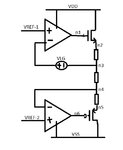
Please see the sketch of my circuit here.
8ZveV2Q.jpg

I want to do loop-gain analysis (a.k.a. loop stability analysis) for the top loop. In simulation I simply put a voltage source (i.e. VLG) in part of the feedback and run the LG analysis (ie. AC loop gain).

My question is how to get my various poles and zeroes when I have multiple feedback loop? Note I'm not asking from simulation point of view but rather from analysis, let's say I need to derive the poles and zeros.

If n4 (node-4) is ground/VSS then this is a simple 1-loop system where my first pole will be at n1 (most likely dominant) and second pole at n2 and that's that. With additional loop at the bottom, I would think that my small signals from VLG will also travel to the bottom loop and thus affecting the overall response. How do I derive the combined transfer function for multiple loop such as this?

My simulation shows a zero appearing but I have no idea where from.

Thank you in advance for all your responses. Have a great day!
 
Last edited by a moderator:

How do I derive the combined transfer function for multiple loop such as this?
You have to calculate the closed loop transfer function by superimposing all branches. You can't predict its poles and zeros by looking at individual loop transfer functions.

For complete stability assessment, the loop gain of each loops has to be checked in the combined circuit.

See also https://www.edaboard.com/showthread.php?125419-Stability-analysis-for-multiple-fedback-loops

I'm not clear about your example, can you give a more visual description, e.g. a schematic.
 

I'm not clear about your example, can you give a more visual description, e.g. a schematic.

The op-amp is a simple 5 transistor op-amp, with gain of around 40-50dB, the total resistor is around 500K Ohm.
My schematic looks almost exactly like the sketch I provided except with values of the resistor & W/L size of the two MOS. What other information do you require? I'll do my best to provide them.

You have to calculate the closed loop transfer function by superimposing all branches.
This is exactly the part that I'm confused about, the derivation of the transfer function. Could you perhaps help me out on how to do this?
For starters, I usually trace starting from the VLG (+ end), it will give out small signals that travel through the circuit and come back around (- end).
So from the VLG+ to n1 would be gm1.Z1 (Z1 = equivalent impedance at opamp output) and then from n1 to n2 would be gm2.Z2. Z1 and Z2 would form my 2 poles (normally) and it will simply be the R1/2 and C1/2 at that nodes. Now, after this is the part that I'm confused about, how to proceed when the small signals arrive at n2. How do I derive the path from n2 to VLG-?
 

What are those little rectangles between n2 and n3, between n3 and n4, and between n4 and n5? Are they resistors, capacitors, inductors, or some combination of those? Show them for what they are, or if you want them to be completely general impedances, at least label them as Z3, Z4, etc. If you must account for capacitances internal to the FETs, indicate them. Do both FETs have the same gm?

To find a transfer function of a circuit, you must decide what is the input (or inputs if differential) and what is the output (or outputs if differential). Are the input(s) voltages or currents? Are the output(s) voltages or currents? Indicate these things on the diagram.

If you want help, you need much more detail than you have given so far.
 

I missed the link in the original post. Please upload schematics with the post, as required by forum rules.

Loop gain analysis has to be performed for both loops. VLG seems like a good place to cut the loop. I personally prefer Middlebrooks method, many references at Edaboard and the rest of the internet. In this case (high impedance OP input, unidirectional signal path), you apply a voltage with VLG and calculate the ratio of the voltages at both sides of VLG which is your loop gain.

Both feedback loops should be stable.

As for the closed loop transfer function, you have to specify in- and outputs, as mentioned by The Electrician.
 

@FvM,

Thank you for the reply. Indeed I am doing exactly what you specified with my simulations, using VLG and middlebrooks method on both loop, measuring ratio on both sides of VLG. The thing is, I see a zero appears on my simulation and I'm trying to figure out where it comes from, so in other words from theoretical/calculation point of view how do I derive where is this zero coming from? My attempt at derivation was stuck when I arrive at n2. I imagine the small signal will split into the 2 loops but have no idea how to express this in derivation.
Basically I'm trying to figure out which components control my zero. I can do trial and error with simulations of course, by varying various components and see if the zero moves, but at best it will give me an educated guess rather than giving me a good understanding of the system, which is what I seek.

@Electrician,
Thanks for the reply. As @Easypeasy mentioned, the rectangles are in fact resistors. Both FET do not have the same gm, we can call it gmn and gmp for those 2 FETs. I think I was mistaken when asking closed-loop TF, rather I'm trying to understand where does a zero comes from on my middlebrooks analysis on VLG.
 

If we abstract from all parasitic elements like MOSFET capacitances, only have a single pole OP and ideal gm, the OP pole translates into a zero in the output impedance of each reference circuit. It shows as a zero in loop gain of the complementary circuit.
 

@FvM,
Can you elaborate more on this please? I don't understand what you mean here.

If I don't have the circuit at the bottom, my VLG Middlebrooks analysis will not show a zero but with the additional loop at the bottom it will, I don't understand why.
 

I presume the simulation will show you what's happening. You have to look at the output impedance of complementary loop and how it affects the loop gain. If you have a LTspice or generic SPICE simulation circuit, why not post it here?
 

@FvM,
Attached is the simulation results for loop gain analysis at VLG.

As you can see there is a zero at around 1-2MHz followed by 2 additional poles afterwards. I'm wondering where this zero is coming from and also the additional 3rd pole.
 

Attachments

  • VLG_typ.JPG
    VLG_typ.JPG
    125.1 KB · Views: 258

Many possible reasons. It's useless to guess about it without the actual simulation circuit and component models.
 

hmmm... I think sharing the simulation models might be problematic for me....
I was hoping that we can approach it in a more generic sense, kinda like analysing the effect of a miller compensation cap in a 2-stage op-amp, the effect on the poles/zeros can be analysed independent of the technology nodes/simulation models used.
Similarly, in this case we have a 5 transistor amplifier followed by a source follower and a string of resistor, is it possible to analyse what happens to the poles/zeros without involving the exact sim models, like the miller case? We can simply use term such as gm1, Ro1 to represent the components.
 

Here is my opinion about what is happening here based on the discussion you guys had above. Say you check the loop stability of the top amplifier. The bottom amplifier presents a pretty low output impedance (looking down into n4) while its loop gain is high. However, the bottom amp output impedance starts to increase with with frequency as its loop gain starts to decrease which is kind of having an inductive behavior for some range of frequencies. So, that effective inductance loads the top stage and will create a zero and a pole, the zero, I think comes first.
 
Last edited:
  • Like
Reactions: komax and FvM

    FvM

    Points: 2
    Helpful Answer Positive Rating

    komax

    Points: 2
    Helpful Answer Positive Rating
@sutapanaki,

Thank you so much for the answer!
Can you help me understand why impedance looking down from n4 is inversely proportional to the loop gain of the bottom loop? Is it from the characteristic of series-shunt feedback config and its effect to Rin/Rout?
 

Sure, due to series-shunt feedback working.
 
  • Like
Reactions: komax

    komax

    Points: 2
    Helpful Answer Positive Rating
@sutapanaki,

Thank you so much for the answer!
Can you help me understand why impedance looking down from n4 is inversely proportional to the loop gain of the bottom loop? Is it from the characteristic of series-shunt feedback config and its effect to Rin/Rout?

Yes, as FvM said, that's the reason. Shunt feedback at the output reduces the impedance but only for as long as the loop gain is high. Once the loop gain dies with frequency, there is nothing else to keep the output impedance low, so it increases. Well, until some load or parasitic capacitors eventually start bringing it down again.

You can do an easy simulation. Simulate the impedance looking down into n4 and then superimpose it on the loop gain of the top amplifier and see what you get. You can also show it here.
 
  • Like
Reactions: komax and FvM

    FvM

    Points: 2
    Helpful Answer Positive Rating

    komax

    Points: 2
    Helpful Answer Positive Rating
@FvM and @sutapanaki,
Thank you both for your answers, much appreciated. I have a better understanding of the system now.
Have a good day!
 

Status
Not open for further replies.

Similar threads

Part and Inventory Search

Welcome to EDABoard.com

Sponsor

Back
Top