Continue to Site

Welcome to EDAboard.com

Welcome to our site! EDAboard.com is an international Electronics Discussion Forum focused on EDA software, circuits, schematics, books, theory, papers, asic, pld, 8051, DSP, Network, RF, Analog Design, PCB, Service Manuals... and a whole lot more! To participate you need to register. Registration is free. Click here to register now.

Inverter SineWave Problem

Status
Not open for further replies.

nihan_A

Newbie level 5
Newbie level 5
Joined
Apr 11, 2018
Messages
8
Helped
1
Reputation
2
Reaction score
0
Trophy points
1
Activity points
131
Hello everyone!

I am trying to remake an inverter which previously designed with IPM. I redesign it with mosfets instead of IPM and I use push-pull topology. I change PWM pulse width while reading the input voltage of the inverter (Such as if input voltage is 60V mosfet is on for 3.5msn-this is minimum pulse- if voltage is lower than 60V pulse increase up to 9msn). Actually I think there is nothing wrong with PWM since if there is load at the ouput there is no problem at all. But if there is no load at the output of inverter my sinewave is not as expected as you can see below

w3.jpeg

But it should be like this:
download.png


It seems like something acts like a capacitor when both of the mosfets are off state. But I don't have any idea.

Here is my schematic
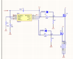
Screenshot_1.png

The U and V points are connected to transformer and center of the transformer is connected to 60V battery as you can see below
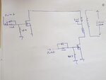
W2.jpeg

I am waiting for you replies.
 

Hi,

It seems like something acts like a capacitor when both of the mosfets are off state. But I don't have any idea.
Not a capacitor, but the inductance of the transformer.

When a MOSFET is active then the transformer is powered. During this time energy is stored in the transformer in form of magnetism.
When you release the MOSFET the stored energy tries to keep the current ... resulting in opposite ouput voltage.
During this phase the (opposite) output voltage is limited by the body diode of the opposite (not the just switched OFF) MOSFET.

Klaus
 
Hi,


Not a capacitor, but the inductance of the transformer.

When a MOSFET is active then the transformer is powered. During this time energy is stored in the transformer in form of magnetism.
When you release the MOSFET the stored energy tries to keep the current ... resulting in opposite ouput voltage.
During this phase the (opposite) output voltage is limited by the body diode of the opposite (not the just switched OFF) MOSFET.

Klaus

Just expectable, you see the energy stored in output transformer.

That is expected then.. So how can I get rid of this opposite output voltage? Since signal is like this my output voltage increase about 300V. And that is not acceptable in my case..
Actually I don't have much experience in power electronics but I googled and some people say just use full bridge topology instead of pushpull but it will be better for me if there is a way out for this problem.
 

Use a base load. Transformer is free-wheeling in this power stage topology, you can't avoid inductive "kick back".

Or use a different topology, e.g. transformer driven by H-bridge.
 
... or the method used by some Chinese inverters: generate about 150V DC from a boost converter then supply it to a H-Bridge with the AC taken from the bridge arms. They do not use an output transformer at all, the AC is basically +150V, 0V, -150V, 0V in sequence giving your modified sine waveform with about 300V p-p.

Brian.
 
But it should be like this:
View attachment 153016

This is a modified sine-wave. Spikes are produced at shut-off, and they are more severe because of going to a high-impedance state.
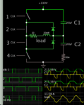
Consider trying a diode-clamped 3-level. It's similar to your push-pull design. It diverts spikes by connecting diodes momentarily across the inductive load.

- - - Updated - - -

diode clamped 3-level 330vdc to series LR load .png

Notice the absence of severe spikes. I made the load semi-inductive, semi-resistive. That could also be the primary of a transformer. Adjust DC supply voltage as needed.
 

when you turn off either of the switching FETs the current in the primary has to find another path
your hand drawn push pull schematic (4 of 4 post 1) does not show anything to provide this path

add a diode across the DS of each FET so the primary current has a path at FET turn off
fast reverse recovery, same current and power capability as FET

(you might be able to get away with diode, because it should conduct for
less time than the FET)

add a capacitor from 60V center tap to ground
 

The diodes don't change anything. Negative DS voltage is already clamped by the substrates diodes, according to the sketched waveform, they are effective.
 

you need a 3rd switch either on the pri or sec to short out the transformer in the dead time between power pulses - else the magnetising current in the Tx at the end of each power pulse will give rise to the extra voltage waveforms you are seeing - as covered by the commenters above
 
  • Like
Reactions: FvM

    FvM

    Points: 2
    Helpful Answer Positive Rating
Status
Not open for further replies.

Similar threads

Part and Inventory Search

Welcome to EDABoard.com

Sponsor

Back
Top