Continue to Site

Welcome to EDAboard.com

Welcome to our site! EDAboard.com is an international Electronics Discussion Forum focused on EDA software, circuits, schematics, books, theory, papers, asic, pld, 8051, DSP, Network, RF, Analog Design, PCB, Service Manuals... and a whole lot more! To participate you need to register. Registration is free. Click here to register now.

[SOLVED] Settling time simulation for the operational amplifier in Cadence

Status
Not open for further replies.

Junus2012

Advanced Member level 5
Joined
Jan 9, 2012
Messages
1,552
Helped
47
Reputation
98
Reaction score
53
Trophy points
1,328
Location
Italy
Activity points
15,235
Dear friends,

I am trying to simulate the Settling time of my operational amplifier. I am connecting it as a unity gain buffer and applying a step input signal.

As far as I believe that settling time is a small signal property, and therefore to simulate it we must sure that the amplifier is not slewing. However, if we see the outputput of the amplifier from any literature they still show the slew part when determining the settling time. Please see the below image from Allen Holberg. Although he was confirming to reduce the input signal step to avoide the slew rate.

Here is my first question please, what is the appropriate input step voltage properties to simulate the Settling time (Step voltage value, Pulse width, Pulse period, delay time, rising and falling time) ?
The second question is how can I know from my output signal that my amplifier is not slewing ? does it mean I should see now slope from high to low or low to high ?
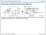
Untitled.png

I also attached you the Settling time function from Cadence calculator to refer to it in your kind explanation

cadence.png

Here I found one file from the internet but he is not explaining why he is taking the chosen value

View attachment settling_gain.pdf

Thank you in advance
 

Settling time is not necessarily a small signal thing. You may simulate settling time for small steps to avoid slewing or you can apply large steps and test your settling with slewing included. In fact, I think you should do both.

The amplitude of the input step for no slewing settling should be small enough not to saturate your input stage, that is small enough not to completely turn off one of the transistors in the diff pair and have all the tail current go through the other one. Which is also one possible way to check if you are not slewing yet. Basically, your feedback returns some voltage to the input, while the other input receives the input step. When you apply the step, the amplifier and hence the fed back signal can not react instantaneously and as a consequence you'll have some initial large delta V at the input. Small step in this case will mean that this initial voltage does not completely saturate the diff pair. It is usually something in the order of sqrt(2)*Vov of the diff pair transistors and to make sure you're doing small signal use a step that produces initial input Vdiff below that value.
Rise/fall time is not that critical - the smaller the better, because you want to approach the ideal step function. But then your amplifier is not going to react to extremely fast rise/fall times, so maybe something like 0.5 to 1ns should be enough (I forgot what was the unity gain BW of your amplifier loop gain).
Pulse width should be enough to show the whole settling of the output.

I don't think you really need that cadence settling time thing. Yes, you want to know how much time the amp takes to settle, but more importantly, you will want to see how it settles - does it ring while settling, does it overshoot and by how much, or does it just settle aperiodically.
 
In Baker's book, CMOS Circuit Design, Layout, and Simulation 3rd ed. pp. 787, for testing he used a 5mV step input signal to avoid slew rate limitations.
 
Last edited:
Settling time is a general parameter and usually it has a sense when the information of accuracy level for settling is provided too.

The division between small and large signal response is a convention, but it is simple and clear.
Small signal approximation is a linearization of the device. So, you can look on the response, and say that as long as the response is following exponential function, it is small signal. When it starts to be a linear function of time, it is large signal response.

The more precise answer is to look on the input and output voltages in respect to operating points of the transistor.
In case of differential pair you can check for which input voltage range, the differential transconductance is constant (or differential current of diff-pair is linear). In the extreme case (no degeneration of diff pair and deep weak inversion, current of MOST diff pair can be approximated to well-known formula for BJT diff-pair), the relation is proportional to tanh(2Vin/Vt), when Vt is a thermal voltage - it can gives you limit for input voltage to keep diff-pair linear. This value is small and we can say that with very good accuracy it is 0.2×Vt (≈5mV). For MOST it is a bit higher limit, however hard to calculated due to non-elementary I-V relationship of MOST.

From the other hand, the OPAMP use to working with closed loop and some gain. For low gain configuration it is not a big deal to not taking care of output amplitude, when input signal is small enough. However, for high gain we can imagine, that 5mV input signal can generate 500mV output step (what can be close to saturation of such OPAMP with below 1V supplies). Here we need to look on the DC OPs of output current sources (or source follower stage if exists), to keep them on the output I-V characteristic point with no large changes in the current (it is relatively easy when are saturated).

The time parameters of the input step are easy to guess.
Input step signal should imitate Heaviside function, so it rise/fall time should be close to 0 in comparison to rise/fall time of response - your OPAMP UGF is 100MHz=628Mrad/s, it means it rise/fall time is ≈1/(2.2×UGF(rad/s))≈720ps, so 10ps should not affect response timing.
The minimum step duration is again simple - 95% is achieved after 3/UGF(rad/s), 99.4% after 5/UGF(rad/s), 10bit accuracy after 10.5/UGF(rad/s). So, depending on your needs you can set the optimum step duration.
The period could be infinity, because you need only one rising and one falling edge.
 
I would be careful about using these textbook small signal
methods if (and this is sometimes the case) the op amp
-is- intended to be used in applications such as unity gain
buffer, DAC follower / current-to-voltage conversion and
the like. Then you -will- have large signal input and you
-will- wind up the input stage momentarily, and you should
care about settling performance under those (application-
realistic) conditions.
 
Dear Friends,

Thank you very much for your kind explanation,

I understood now how to apply a step signal signal and still in the linear region by monitoring the current of my differential pair transistors. I applied 10 mV and still at the transition time both of the transistors are ON. The setting of my source is shown below after considering your explanation

source setting.png

I rub the transient to see only the low to high settling time (same should be applied to see the high to low settling time). Kindly see the result below

result.png

I am using fully differential amplifier with GBW = 20 MHz with unity gain connection. I applied differential input step (one opposite to other) and the taken output is the VOD (differential output voltage VO+-VO-)
The phase margin of my circuit is 80 Degree therefore you will not see some bounce at the transition time.

From hand calculation I can easily see that my Settling time is (2 us-2.0388 us) which is equal to 38.8 ns.

However if I use the calculator tool from cadence is giving me such huge value as 2 us.

I would show you my calculator setting below

calce.png

Hope to hear from your opinions,
 

Calculator gives correct value. It is the absolute settling time, not the relative. It means it gives back the time value when the signal is settled, which should be after 2us definitely if the excitation happens at 2us.
Subtract the 2us from the calculated value to get the relative settling time.
 
  • Like
Reactions: Junus2012

    V

    Points: 2
    Helpful Answer Positive Rating

    Junus2012

    Points: 2
    Helpful Answer Positive Rating
Dear Frankrose,

Thank you very much for your reply.

Yes you are right, because I gave a delay time of 2 us, so I must subtract it, then the result of the settling time of the amp from the calculator is about 21 ns as you can see from the image below

result2.png

Does it good value in your opinion ?

Now if I would like to give the settling time but for large input signal, I can simply add this value (21 ns) to the slew rate duration value.

Thank you a lot
 

Your UGBW=20MHz, which for unity feedback configuration results in tau equal to about 8ns. Now, it depends on the accuracy to which you want to settle. If you want 6 bit of accuracy you need about 5 tau, which is about 40ns. 10 bit accuracy is about 8 tau or 64ns.

If you stimulate with a large input step, you'll get settling that includes both slewing and linear settling.

Dear all friends, Thank you for your kind help,


I would like to ask you about the simulation setup for simulating the slew rate or the settling time, usually I see from Holberg and Jakob they use only positive voltage above the the common mode voltage (VCM). for example in Jakob he use 1 v single supply operation, then he apply positive pulse voltage above 0.5 (which is the VCM in his case). However, I follow any company procedure I see they will apply a voltage that is allowed by the ICMR above and below the VCM, not only above the VCM.

if I follow the procedure of Jakob or the Holberg I will lose the half of my slew rate real value. This make me confused
 

Thank you Suta for confirming me..

Now I would like to ask you about the settling accuracy relationship with the bit accuracy.

if I am reading the settling time with 5% error band, how much this equal to bit accuracy ? what is the formula for it ?

in the company data sheet they usually specify the error percentage with 0.1% or less. However in cadence calculator it is not allowing me to simulate with less than 1%.

Thank you once again
 

For data Converters accuracy is set by 0.5 LSB. It means, V_FS./2^(N+1), where V_FS is a full scale amplitude and N is a resolution. To get percentage value you need to normalize it to V_FS. I. E. 5% is equivalent to 3.3 bits

A few posts above you have shown the ViVa calculator result for settling with 0.1% settling time accuracy, so your statement seems to be incorrect.
 
Thank you Suta for confirming me..

Now I would like to ask you about the settling accuracy relationship with the bit accuracy.

if I am reading the settling time with 5% error band, how much this equal to bit accuracy ? what is the formula for it ?

in the company data sheet they usually specify the error percentage with 0.1% or less. However in cadence calculator it is not allowing me to simulate with less than 1%.

Thank you once again

The post above from Dominik explains it well. Basically, accuracy converted to bits is the equivalent ADC's LSB with respect to full scale (or 0.5 LSB - more stringent). 0.1% is 1/1000 which means sort of 1/1000 of the full scale, similar to a 10 bit resolution, because you can imagine an ADC with 1v full scale and 1024 LSBs. In other words 1/1000 is kind of same as 1/1024.
 
Dear Dominik
Deasr Suta

Thank you very much for your explanation... you made my last statement clear, now I understand what you mean by settling time accuracy given in term of bits as an equivelant or other expression for the accuracy error percentage.

This will makes me go forward in my questions :) and I hope I am not making the posts boring :)

dear Dominic

you presented this expressions in you past post,

rise/fall time is ≈1/(2.2×UGF(rad/s))
The minimum step duration is again simple - 95% is achieved after 3/UGF(rad/s), 99.4% after 5/UGF(rad/s), 10bit accuracy after 10.5/UGF(rad/s)

can you please provide me with the reference about it so I can study more details about it ?

Dear Suta,

you presented this expression before,

If you want 6 bit of accuracy you need about 5 tau, which is about 40ns. 10 bit accuracy is about 8 tau or 64ns.

It will be very kind of you if you also provide me with the reference to study it more

Thank you very much once again
 

I don't have a reference off the top of my head. I think you can find this in any book that deals with data converters. But the reasoning is like this. Imagine a simple model of S/H circuit - just a resistor and then a capacitor to ground and you take the output across the capacitor. The input of this divider is the full scale voltage of the ADC (or your step). Initial conditions on the capacitor are zero. Then you step in the input to VFS (full scale voltage). The settling is simple exponential

Vout=VFS(1-exp(-t/tau))

We want to know the error at some time Ts. This is of course

|Vout,error| = |VFS|exp(-Ts/tau)=|VFS|exp(-N)

where N is the number of time constants tau that fit into Ts

We need 0.5LSB accuracy, which is VFS/(2*2^B) where B-number of bits

Finding N=ln(2*2^B)

If B=10 for a 10 bit ADC we need N>=ln(2*2^10)=7.6 time constants
 
Last edited:
Dear friends,

Thank you very much for your help

I have noticed one thing after I learned the setup from you about the settling time. I went back to my slew rate simulation and I corrected the rising and falling time of the input signal. In the past I was using 1 ns for tr&tf and now 50 Ps. Now the slew rate I am reading is 120 v/us rather than 80 v/us from before. is it logical to get this change ?
remember please that my settling time is about 28 ns and the GBW is 20 MHz

Thank you very much
 

Did you compare how much differential input voltage you have initially for the case of 1ns and 50ps? Respectively, does all the tail current goes only in one side of the diff pair for both cases?
 
Dear Suta,

I am applying the same input differential pulse voltage for the both cases which is +-0.5Vp (maximum ICMR in my design).
For the tail current if it is going in to one side I will check it next time when I go to Lab.

So I think you want to say that when I was applying my pulse signal with 1 ns rising and falling edge perhaps not all the current is going in one side as it is happeing now with the casse of 50 tr&tf of 50 Ps.

If I go back to Dominik formula some post above he gave an estimation for the rising and falling time of the op-amp itself as :

rise/fall time is ≈1/(2.2×UGF(rad/s))............. for 20 MHz for my design then tr&tf = 3.6 n s,,,,,, it means the 1 ns was not samll enogh comapring to 3.6 ns and hence getting not right result.

That is only on the hope if I am right

Thank you once again
 

Well, UGF is a small signal parameter. Slewing is something relating to large signals, although there is a relation between SR and UGF.
 
Status
Not open for further replies.

Part and Inventory Search

Welcome to EDABoard.com

Sponsor

Back
Top