Continue to Site

Welcome to EDAboard.com

Welcome to our site! EDAboard.com is an international Electronics Discussion Forum focused on EDA software, circuits, schematics, books, theory, papers, asic, pld, 8051, DSP, Network, RF, Analog Design, PCB, Service Manuals... and a whole lot more! To participate you need to register. Registration is free. Click here to register now.

[SOLVED] Via Ground in ADS for connecting source of transistor to ground

Status
Not open for further replies.

Antra_Saxena

Newbie level 4
Newbie level 4
Joined
Feb 20, 2019
Messages
6
Helped
0
Reputation
0
Reaction score
0
Trophy points
1
Activity points
51
Hello,

I am designing a PA using Cree transistor.

When I am doing EM simulation, after optimization of full PA ( EM model), I am getting PAE of 67%. Then, I observed that I have ideal ground in EM simulation at the source of the transistor. When I replaced it with Via ground, after optimization I can achieve up to 55 % only.

I am not understanding, why one Via ground reduced my PAE drastically.
Is it necessary to have Via ground or ideal ground can work?

When soldering a Cree transistor, source need to be connected to ground, via ground is required?


Thanks in advance,
 

Via to ground and it's dimensions will affect characteristics of amplifier. You may plot s-parameters for different via sizes and see the difference.
What Cree transistor do you use? If it is soldered you may try coplanar-style layout with many vias.
 

In order to improve the efficiency, you have to place many VIAs in parallel to reduce the total inductance.( and resistance too)
Because small inductance+resistance will effect the operation of the PA being as "negative feedback" and it's extremely important in PA Designs due to high current.
 

Thanks for your reply.
CGH40010F- Cree transistor

What size of Via I should use to reduce the error in terms of efficiency?

- - - Updated - - -

Thank you for your reply.

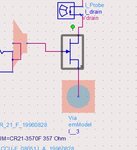
I am attaching the screenshot of my design. Should I place these Vias in parallel?
I checked the datasheet of the Cree transistor. The width of the source is 155 mil. So, how many Vias can I put in parallel? Cree1.JPG
 

Ah, I used that transistor before. Nice for high power applications. Although, it have some stability issues, so be careful of that.

You gotta simulate for different via dimaters along the source. Via size also differs from substrate selection. Create different stackups and test for all of them to find which one suits you. Ro4003C or Ro4350B will have different behaviors. Check for current density graphics in HFSS or ADS, and see if your via is useful in conducting current.
 

Status
Not open for further replies.

Part and Inventory Search

Welcome to EDABoard.com

Sponsor

Back
Top