Continue to Site

Welcome to EDAboard.com

Welcome to our site! EDAboard.com is an international Electronics Discussion Forum focused on EDA software, circuits, schematics, books, theory, papers, asic, pld, 8051, DSP, Network, RF, Analog Design, PCB, Service Manuals... and a whole lot more! To participate you need to register. Registration is free. Click here to register now.

Converting series-through s-parameter measurements to shunt configuration (ADS)

Status
Not open for further replies.

seackone

Junior Member level 1
Joined
Feb 9, 2018
Messages
19
Helped
0
Reputation
0
Reaction score
0
Trophy points
1
Activity points
248
Hi,
I measured a voltage controlled capacitor with a network analyzer (NWA) in series-through configuration. That means: Port 1 of the NWA is connected with RF input of the capacitor, Port 2 accordingly with the output. For every capacitor bias voltage (1 V to 24 V with 0.1 V steps), i've got one 2 Port s-parameter file.

After that, I want to implement these files in Keysight's "Advanced Design System" (ADS) to calculate the capacity over bias voltage for different frequencies. There is no problem with a 50 ohm term element at the start and the end of the s-parameter container (which contains the measured s-parameter files) and a simple s-parameter simulation. Thats configuration is equal to the measurement with the NWA.

Now, I want to simulate the capacitor in shunt configuration (RF input with 50 ohm term element, output connected to ground). Is there any possibility to use my series-through s-parameter measurement (50 Ohm at the two ports) for the shunt simulation without measuring the capacitor again? Maybe with an equivalent subcircuit or something else?

Thank you for your ideas.

Best regards.
 

Now, I want to simulate the capacitor in shunt configuration (RF input with 50 ohm term element, output connected to ground). Is there any possibility to use my series-through s-parameter measurement (50 Ohm at the two ports) for the shunt simulation without measuring the capacitor again? Maybe with an equivalent subcircuit or something else?

It's less complicated than you think. The 2-port S-parameters are measured with 50 Ohm at the ports, but when used in the circuit simulator, the simulator takes care of calculating currents & voltages for the actual load, so simulation results are valid for all possible terminations.

The simplest solution is to place an ADS ground at one of the S2P ports. For more accurate results, you might want to include the parasitics (series L, series R) in that ground path, so look for the microstrip via element in ADS.

PS: What I wrote above assumes that your S2P data is for the SMD device only, properly calibrated at the SMD reference planes, and there is no extra feedline length included in the measured data.
 
Vielen Dank für Ihre Antwort Herr Dr. Mühlhaus!

Okay, let's write in english again. But it's not really easy since I know, there is an other german who's answering to my questions. It's a pleasure to get help of an expert in ADS, thank you very much!

At first:
I designed a 50 Ohm stripline for the SMA to capacitor connection (and let produced that PCB of course). The calibration reference plane is at the end of the NWA's connection cables but shifted to the capacitor by using the "port extensions" - setting of the NWA (unfortunately I missed to let produce more PCBs with short, open and load termination for a calibration directly at the capacitors ports).

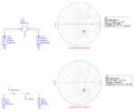
At the beginning of my simulation, I used these s-parameter files in series configuration and compared that results with an ideal capacitor and a series resistor. I hope these comparison is allowed? You can see the results in Picture 1. The simulation is at 850 MHz and 2 V bias voltage of the capacitor and corresponds to a 3.56 pF capacity (nearly the same value as specified in the datasheet)

Picture1.png

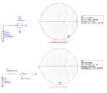
After that, I tried exactly what you wrote in your reply (with exception of including the parasitics): I simply connect the output of the capacitor to ground. You can see the results in picture 2. I've got a negative real part and a capacity of 2.12 pF.

Picture2.png

I used your hint with adding a stripline between the output of the capacitor and the connection to ground. With optimization and goals, I figured out the length and width of the stripline to match the equivalent ideal capacitor in shunt configuration. But that's just a solution for one frequency or bias voltage of the real capacitor. I tested with at different frequencies and voltages (with the calculated stripline between output and ground) but got no satisfying result.

During I type this message, I'm thinking about another measurement:

What if I'm using the NWA's calibration plane at the end of the cables and adding the momentum simulation of the PCB at the beginning and end of my s2p container in the simulation?

Is it permissable at all to compare my measurements with an ideal capacitor (with the additional resistor) to get an equivalent subcircuit (by adding a stripline between output and ground for example)?

Best regards
 

Once you obtain s-parameters, there should be no problem using in shunt or series configuration. Make a quick test, measure two port s-parameters of a series capacitor in ADS like you did it in network analyzer. Then, measure two port s-parameters using the s-parameter file in shunt configuration. Measure the actual capacitor in shunt configuration, compare the results. You will make sure whether an s-parameter block can be used regardless of configuration.

I have just posted my comments, your questions are still up.
 

Hello,

The calibration reference plane is at the end of the NWA's connection cables but shifted to the capacitor by using the "port extensions" - setting of the NWA (unfortunately I missed to let produce more PCBs with short, open and load termination for a calibration directly at the capacitors ports).

Ok, at last the ref planes are approximately at the component pads. In the past, I used TRL calibration with homebrew line standards on the actual PCB material for really accurate results. Then, you know exactly the reference position (outer end of pad, for example) and what parasitics are already included (pad size ___ or via ___ on substrate ___).

At the beginning of my simulation, I used these s-parameter files in series configuration and compared that results with an ideal capacitor and a series resistor. I hope these comparison is allowed?

No problem, this approach is fine for series C extraction at low frequency. At high frequency, physical size of the C causes series L -> self resonance frequency, and that depends on the reference planes where you define your component: between inside of pads, or pad center, or outer pad edges? Also , the shunt capacitance of the pads is included and might have a visible effect.

After that, I tried exactly what you wrote in your reply (with exception of including the parasitics): I simply connect the output of the capacitor to ground. You can see the results in picture 2. I've got a negative real part and a capacity of 2.12 pF.

The negative real part should not bere there, of course, so there is some issue with your measurement data. One issue might be that you used ref plane shift, which only adjusts the phase but doesn't remove the loss of the PCB feedline.

I used your hint with adding a stripline between the output of the capacitor and the connection to ground. With optimization and goals, I figured out the length and width of the stripline to match the equivalent ideal capacitor in shunt configuration. But that's just a solution for one frequency or bias voltage of the real capacitor. I tested with at different frequencies and voltages (with the calculated stripline between output and ground) but got no satisfying result.

Just to avoid a misunderstanding: I meant the extra length that is added if you physically ground the capacitor on the PCB. That said, there is also some length in your SMD C measurement that might not be removed properly in the data. I would replace the C by a known object (0 Ohm thru) and test that. Then you should only have 0 Ohm with some series inductance from the length of the thru.

During I type this message, I'm thinking about another measurement:

What if I'm using the NWA's calibration plane at the end of the cables and adding the momentum simulation of the PCB at the beginning and end of my s2p container in the simulation?

I would prefer TRL calibration as described above, where the SMD-to-PCB transition and the feedline on PCB can be accurately removed.
If your primary goal is to get the bias-dependent change in C, then you might tweak your existing setup to give reasonable results for the 0 Ohm jumper, and then go from there.

Is it permissable at all to compare my measurements with an ideal capacitor (with the additional resistor) to get an equivalent subcircuit (by adding a stripline between output and ground for example)?

Series R + C + L should be ok. The series L is to model the finite size of the device, but your proposal for microstrip model instead of lumped L is even better.
 
Thank you for your answer. Okay, I didn't know that it should be so easy to simulate a s2p file to ground if my DUT was measured with 50 ohm termination at both ports.

But you can see, there is a big difference between the s2p simulation in series configuration (upper simulation in picture one) and in shunt configuration (upper simulation in picture two). Apart from the real part, the imaginary part should be the same. But I have a difference of more than 1.2 pF of the capacitor between these two simulations. I think thats caused by some parasitics but i couldn't figure out how to optimize my schematic for an universal solution (that mean for different frequencies and bias voltages).

- - - Updated - - -

Sorry, my last answer was under review by a moderator during you replied.

Okay, want to measure the capacitor next monday again. I have two pcbs left without any components. It should be possible to make an own TRL calibration for an exact measurement of the capacitor.

Thank you for your help, I will post my results next week!
 

But you can see, there is a big difference between the s2p simulation in series configuration (upper simulation in picture one) and in shunt configuration (upper simulation in picture two). Apart from the real part, the imaginary part should be the same.

I disagree. Your measured SMD device has series and shunt path components, and this leads to different results in series and shunt configuration. Have a look at my appnote
https://muehlhaus.com/support/ads-application-notes/inductor-em-ports
See section "Why are these results different"
 
PS: Or do you refer to the different locations in the Smith chart in your testcase? :shock:
That is expected and correct, because one results is for RC connected to ground, and the other result is for RC in series with the port 2 load (50 Ohm).
 

Your measured SMD device has series and shunt path components, and this leads to different results in series and shunt configuration.

Very impressive article, absolutely comprehensibly. Especially with the sketch! Thank you very much.

That there are different locations in the smith chart is what I expected (on the basis of the different terminations). Apart from the real part (series R, okay negative... I would measure tomorrow again with a new calibration), I thought i get the same imaginary part to calculate the capacity:

C = 1/(2*pi*f*Xc)

f = frequency (in the example above 850*10^6 Hz)
Xc = Imaginary part normalized to 50 Ohm (-88.453 Ohm)

That means, if I want to compare a capacitor in shunt and series configuration (at the same frequency), I always get a different capacity (causes by the series and shunt path components of the device)?

Hm. Its plausible. The datasheet of the voltage controlled capacitor got a capacity to bias voltage diagram.. there is no word about they measured the capacitor in shunt or series configuration (although there is a layout pictured with both configurations). My measured capacity vs. bias voltage is nearly the same as in the datasheet, so I think their diagram is also measured in series configuration.

- - - Updated - - -

I simulated with the real capacitor and the s2p file of the manufacturer in series and shunt configuration again. The imaginary part wasn't the same, but there was a difference of just 1 Ohm. In my measurements with series configuration and simulation of the capacitor connected to ground (picture 1, first illustration and picture 2, first illustration), there is a difference of nearly 35 Ohm of the imaginary part. Is that big difference plausible or caused by a failure of my measurements?
 

One port shouldn't be short circuited to GND in series component measurements because you do short circuit terminal capacitance.Instead, simple two port measurement will be more accurate.
Then you can extract inductance/capacitance values from s-parameters.
Note: Pay attention to Phase Calibration of VNA.Use a equivalent PCB Calibration Test Board if it's available.
 

That means, if I want to compare a capacitor in shunt and series configuration (at the same frequency), I always get a different capacity (causes by the series and shunt path components of the device)?

Yes, and don't forget the SMD pad shunt capacitance!

Example:
Your device has C=3pF and each pad has 1pF.

In 2 port configuration, the effective series capacitance is 3pF + two pads in series = 3.5pF
In 1 port configuration, the effective capacitance to ground is 3pF + one pad = 4pF

there is a difference of nearly 35 Ohm of the imaginary part.

That's a large difference, possibly from error in reference planes (-> extra length). 35 Ohm capacitive or inductive? What is the equivalent L or C?
 

Status
Not open for further replies.

Part and Inventory Search

Welcome to EDABoard.com

Sponsor

Back
Top