Continue to Site

Welcome to EDAboard.com

Welcome to our site! EDAboard.com is an international Electronics Discussion Forum focused on EDA software, circuits, schematics, books, theory, papers, asic, pld, 8051, DSP, Network, RF, Analog Design, PCB, Service Manuals... and a whole lot more! To participate you need to register. Registration is free. Click here to register now.

[SOLVED] Type III compensation

Status
Not open for further replies.

shomikc

Member level 4
Member level 4
Joined
Apr 19, 2013
Messages
71
Helped
0
Reputation
0
Reaction score
0
Trophy points
1,286
Activity points
1,953
Hello all,

I am beginning to think that PID control or any feedback control of power electronics converters is just magic and can only be performed by magicians.

I have tried as a last attempt Type III compensation (PID) but the op-amp output is still saturated at Vcc.
Type III compensation.jpg

Type III compensation ouput.jpg

I followed all the formulas given in https://www.intersil.com/content/dam/Intersil/documents/tb41/tb417.pdf

Please help.

Thank you.

Shomik
 

You have no DC feedback in the op-amp. Basically you have it configured as a comparator, input versus 5V. The schematics in the data sheet are not practical examples, they are only to show the feedback paths and compensation calculations. Try adding a resistor between the output and inverting inputs to restore some linearity.

Brian.
 
Try adding a resistor between the output and inverting inputs to restore some linearity.

Brian.

Do you mean a resistor in parallel to the already existing two parallel paths : one containing R2 and C2 and another containing C3.
 

There's no actual feedback loop in your schematic. The PWM is generated with fixed duty cycle.

Come back with a reasonable feedback topology.

- - - Updated - - -

I see that you have already posted PWM controllers with feedback. Apparently you are missing a basic understanding how I-controllers can be simulated.

Without some kind of negative feedback, they'll always run into saturation. Even if you want to "measure" the open loop gain, there must be an auxiliary DC feedback to setup a stable operation point.
 
I agree with all posts above, but I am missing something as well. Why manufacturers do not provide DC feedback in their working evaluation boards? e.g. this one by Infineon using the IR3840.
There are hundreds from all manufacturers. The Error Amplifier they are using in the IC is different than an OP amp ?
 

Brian, please see page 21 of the IR3840 datasheet. FB is the inverting input of the error amplifier. https://www.infineon.com/dgdl/ir3840m.pdf?fileId=5546d462533600a4015355d2133317d1

- - - Updated - - -

I have figured it out. When the converter is operated in closed loop, the compensator does NOT need any DC feedback, in other words, the compensators referenced in post #1 from Intersil and the one used in the evaluation board referenced in post #5, are all correct, no additional resistance needed.

The problem with post #1 is that he has the Buck converter operating in open loop. Once he closes the loop, the OP Amp will not be saturated anymore without using any DC Feedback.
Since post #1 is using a fixed duty cycle, the error between reference voltage and the divided output voltage will always lead to saturation. If post #1 finishes closing the feedback with PWM modulator, the Op Amp will not be saturated anymore because the DC error will be a value in the order of the Open Loop gain of the OP Amp^(-1) (ideally zero for an ideal OP Amp), he will only see variations because of the ripple i.e. AC voltage.

FvM already addressed this in post #4.
 
Last edited:
  • Like
Reactions: shomikc and FvM

    FvM

    Points: 2
    Helpful Answer Positive Rating

    shomikc

    Points: 2
    Helpful Answer Positive Rating
Dear Sir,

Thanks to you and Mr. Brian for all your help.

I made another circuit with Type III compensator.

VMC Buck in CCM with Type III Compensator.jpg

and the Output voltage waveform looks like this

Output Voltage of VMC Buck in CCM with Type III Compensator.jpg

So what I want to know is what I have done correct. And if it is alright then how and why? I guess I would like to know how it is working? How all the components are behaving individually and as a whole to make the compensation possible.

Thank you.
 

The results I get with your compensation values, shows instability.

When I increase C5 to 470 nF and reduce R10 to 220 Ω, it seems to quiet down (plot 2/3).
 

Attachments

  • loop_unstable.png
    loop_unstable.png
    33.2 KB · Views: 234
Post #8 results does not make sense because the output settles to ~5.8 instead of 2.85V.
e-desing's results shows output voltage when stable ~2.8V which is correct.

@shomikc, please get rid of E2 in addition to correcting feedback loop. You had it O.K. like in post #1 with the voltage divider.
 
Depending on the specific PWM controller/circuit you use it may have a soft-start option feature to prevent overshoot at power on.

Below shows how you can have a dangerous overshoot without soft-start.
 

Attachments

  • soft_strt.png
    soft_strt.png
    18.8 KB · Views: 211
Dear Sir,
Can I ask what software you are using?
Thank you,
Shomik Chakraborty.
 

The compensator circuit itself doesn't need local DC feedback but the entire loop including the modulator and the resistor divider of the output IS dc feedback. DC feedback at the compensator would only serve to cap the DC open-loop gain and there is little reason to do that.

I'm wondering why no one has suggested or asked for bode plots of the compensator. Very simply we want to see a ~45 degree phase boost from the TYPE III compensator around the frequency of the output LC filter.

LTSpice is extremely efficient at doing such a simulation (no experience with PSPICE). When I'm studying feedback I'd use an ideal opamp in the compensator and study the compensator's properties as mentioned above. Then I'd also add the LC filter directly to the output of that ideal compensator as a way to study the entire open loop gain. This leaves out the modulation and assumes that the switching frequency is sufficiently fast the modulation doesn't contribute much phase shift at the desired loop bandwidth which is often true enough.

Though you want to get the gain right: compensator output voltage -> duty cycle -> nominal output voltage -> divided down FB pin voltage is the open loop gain. I.E. for example maybe: 2.5V compensator output -> 50% modulator duty cycle -> 6V nominal output voltage -> 2V divided down FB pin voltage. That example has a 2.5V:2V DC gain from the compensators perspective. So you'd want to input that into the loop somewhere as it directly impacts the bode plots crossover frequency.


I'll also mention PSIM. Spice tools are very good at AC analysis of linear systems but arn't generally realistic for doing AC analysis of switching supplies. PSIM is a good compromise because it specializes in power topology simulation but with ideal switches which allows effective AC analysis of the entire system with the switching modulator. The free version of PSIM is probably good enough for analyzing this system and note that PSIM has a TYPE III compensator block where you simply input the two poles and two zero frequencies. That gets you going very quickly and you can make it a separate task to design an opamp based circuit that matches those properties.
 

Hello all,

I am posting the frequency analysis done here with Matlab.View attachment VMC_Buck.txt

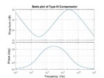
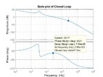
Now to calculate the values a certain K factor has been used which to be set between 0.6 and 1.5. I have set this value to 0.9 and calculated the values of the components of the compensator but I get relevant Bode plots only when I set the output Capacitor as 1000uF.vmc_buck_Bode of Type III Compensator.jpg

vmc_buck_Bode plot of Closed Loop.jpg

And the maximum phase margin I can get is only 68.

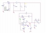
But using Orcad Pspice and the same values for the compensator as calculated in Matlab but I get a result only if my Output Capacitor is 4.7 uF.

latest_vm_buck.jpg

output_latest_vm_buck.jpg

So which value of Output Capacitor do I choose, or rather which of simulations, is wrong / correct?

Also if I use the same values of the compensator calculated in Matlab will it work in practice with SG3524. Please help.
 

Status
Not open for further replies.

Similar threads

Part and Inventory Search

Welcome to EDABoard.com

Sponsor

Back
Top