Continue to Site

Welcome to EDAboard.com

Welcome to our site! EDAboard.com is an international Electronics Discussion Forum focused on EDA software, circuits, schematics, books, theory, papers, asic, pld, 8051, DSP, Network, RF, Analog Design, PCB, Service Manuals... and a whole lot more! To participate you need to register. Registration is free. Click here to register now.

[SOLVED] Low Dropout Voltage Regulator (LDO) design

Status
Not open for further replies.

J.Yuan

Junior Member level 1
Joined
Nov 30, 2017
Messages
15
Helped
1
Reputation
2
Reaction score
1
Trophy points
3
Activity points
107
Hello,

Can anyone suggest the possible value of current source, Vref, VDD, R1, R2, Cload and Rload to me.
Because I trying to run a simulation on cadence software based on LDO design.

Thanks.
 

Attachments

  • LDO.jpg
    LDO.jpg
    14.1 KB · Views: 988
  • LDO.jpg
    LDO.jpg
    14.1 KB · Views: 557
Last edited:

Hi,

I think, from the little I understand, the question is relative to several parameters not provided. What power can the LDO draw? That will affect the current source value.

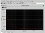
Vref is whatever you want it to be. R1 and R2 divide down V out to match Vref. R1 and R2 can be calculated from the formula in the little blue text box at the top right of the simulation screenshot. I hopew that's what you meant.

R load will depend on the power you give the LDO and its limitations. Aiming for 3.3V, I get ~3.295V with a 1k load in my simulation - it can output a feeble 3mA (the rest of the current drawn on VS1 is regulator operation). C load maybe has to do with stability, and I think I remember the larger the Cload the greater the stability, but the slower the response.

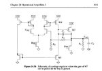
The screenshot is a simulation of a bog-standard regulator copied from a CMOS version - the other image attached. It's BJT's instead of CMOS design, but that's not really here nor there.

vreg values snapshot.JPG vreg schematic cmos book p815.JPG
 
  • Like
Reactions: J.Yuan

    J.Yuan

    Points: 2
    Helpful Answer Positive Rating
What you ask for are "design-to" application values for
the most part. Product definition. If nobody has these
for you then suggest you make up some stuff that is
credible.

Cload will be what makes output transient accuracy
"good enough" for the powered load (an active device
with its own attributes) on load-step events. Rload
(or Iload, depending on load behavior) has to assume
min and max levels. Vout, same deal. Pick a job, any
job, and all of this unfolds.
 
  • Like
Reactions: J.Yuan

    J.Yuan

    Points: 2
    Helpful Answer Positive Rating
Hi,

I think, from the little I understand, the question is relative to several parameters not provided. What power can the LDO draw? That will affect the current source value.

Vref is whatever you want it to be. R1 and R2 divide down V out to match Vref. R1 and R2 can be calculated from the formula in the little blue text box at the top right of the simulation screenshot. I hopew that's what you meant.

R load will depend on the power you give the LDO and its limitations. Aiming for 3.3V, I get ~3.295V with a 1k load in my simulation - it can output a feeble 3mA (the rest of the current drawn on VS1 is regulator operation). C load maybe has to do with stability, and I think I remember the larger the Cload the greater the stability, but the slower the response.

The screenshot is a simulation of a bog-standard regulator copied from a CMOS version - the other image attached. It's BJT's instead of CMOS design, but that's not really here nor there.

View attachment 142974 View attachment 142973

Thanks for answering my question.

I try to design a LDO.
With these parameter:

current sorce= 100uA
Vref= 1.8V
Vdd= 2V
R1= 1K
R2= 11K
Cload= 20pF
Rlaod=1K

it there any wrong?

- - - Updated - - -

What you ask for are "design-to" application values for
the most part. Product definition. If nobody has these
for you then suggest you make up some stuff that is
credible.

Cload will be what makes output transient accuracy
"good enough" for the powered load (an active device
with its own attributes) on load-step events. Rload
(or Iload, depending on load behavior) has to assume
min and max levels. Vout, same deal. Pick a job, any
job, and all of this unfolds.

Thanks for relying me.

this design is used for simulation purpose with 0.18um technology.
because i try to simulate with some value, and I was not able to get desired output.
 

Hi,

Unless I'm mistaken or you have written R1 and R2 values wrong:
R1= 1K, R2= 11K, Vref 1.8V, VDD = 2V. I do not know much about this, nothing about CMOS design but anyway, that seems a high Vref to me, and I think you'd need to be clear about what is the LDO dropout voltage for that design with those MOS.

I say the above because a quick calculation gets me here:

1/(11k/12k = 0.91666666666666666666666666666667)
= 1.0909090909090909090909090909091 * 1.8
= 1.964 V out

I see little point in an LDO that has an output that is virtually the same as the input voltage but I admit I guess there is a reason for this being needed.

Why is Vref so high? It's personal interest as I will learn something. I always want to aim for as low as possible, like a Vbe or similar.

Have you played around with the current source value to see how it affects the I out the regulator can carry?

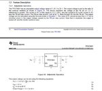
This screenshot from an LDO datasheet shows a more complete calculation for V out, maybe it's applicable to your design.
TPS73801 Vout formula.JPG

If you haven't already and you have access to, or can read it as a Google book, try CMOS Circuit Design Layout and Simulatio 3rd Edition, pages 812 to around 816 or 817ish, it discusses the regulator design, which looks the same as yours, basically, and I at least found it insightful.

N.B. in my schematic using off the shelf parts, ignore the JFET and BJT Vbias thing, it was an experiment tagged onto the bona fide regulator design that does not work as is, I had to use a voltage source to simulate the Vbias of 0.5V.

- - - Updated - - -

Hi again,

Nearly forgot...

How are you generating Vref? Is it stable over load changes, etc.?

It might be that your NMOS current sinks are shapeshifters that will drive you crazy, all being attached to the same source. I found with basic op amp design simulations - from memory - I ended up separating off the tail from the output or other methods/designs to avoid "shapeshifters". Have you probed the simulation to see what's happening down there with the load attached? If you look at the version I copied from that book, a big difference is that the tail bias is not connected to the current bias.
 

Hi and Thanks,
you are nice person for helping me find reference.

In my simulation, the Vref directly using a voltage source. it is a fixed value.
I areadly read the book (pg810-817) you suggest.
I still do not really understand. Because this is my frist time design a LDO circuit.
For calculation, I think your calculation are right, becasue I dont have strong basis knowledge to LDO design.

Based on my LDO design(used in portable device),
Do u mind teach me some formula about LDO? (now, i only know the formula Vout=Vref*(1+(R1/R2)).
what is suitable of Vref ?
May I know Vref and Vdd, which one is input voltage in my design?
 
  • Like
Reactions: d123

    d123

    Points: 2
    Helpful Answer Positive Rating
Hi J.Yuan,

Are you asking about VDD and Vref? If so, VDD is the input voltage. Vref is the comparison voltage for the feedback.

Hate to ask another question, but have you got enough headroom to operate that LDO? I know some can function with 36mV dropout and less, depending on the load.

I would love to help you, really, that's what forums are for. However, it would be dishonest - not to say incredibly deluded - of me to think I am able to share more than I have with you. Remember, I know nothing about CMOS design, I just "play" with circuit designs and so on. Members like dick_freebird and others who work on IC design are able to provide you with real knowledge and answer your questions, I'm just a hobbyist who bungles his way through circuits until they work enough for purpose.

Here are a couple of LDO specific app notes, maybe they'll help/be of interest.

View attachment ldo_concepts.pdfView attachment Topic 9 - Understanding LDO dropout.pdfView attachment Technical Review of Low Dropout Voltage Regulator Operation and Performance slva072 TI.pdf
 

Hi again.

Vref is usually a bandgap, 1.22V. But that's relative, there are sub 1V references in CMOS. When the site is working properly again I'll upload a rar file for you with pretty much all the voltage reference/bandgap stuff I have.

- - - Updated - - -

There we are. I think some is useful, some very, some just of interest, and a couple of datasheets of devices that interested me. If you focus on the ones with bandgap in the title you'll go quicker - if any of it's of any use to you.

View attachment Voltage reference info eda.rar
 

Many newer digital process nodes have core voltages
below 1V and so sub-bandgap (or divided-bandgap)
references are required. You don't want an amplifier's
delay on the feedback, error amp is problem enough
in regard to load step response.

Work the task from back to front. Begin with the
pass element. PMOS if you have a single available
supply and don't want a charge pump making
noise internally. NMOS if you're working at 1V
but have a handy 3.3-5V supply for the gate
drive (see this in all of the "ULDO" types pretty
much). Gate drive path need not be power path
and may be better off, not.

Your pass element needs to deliver comfortably
more than spec rec max current and satisfy any
similar loading in performance specs and known
applications, with comfortably less drive than
min supply-gnd and maximum needed working
headroom in the gate driver will deliver. You also
need to be able to reliably choke output current
to min load spec / test / application with more
Vgs residual, than the gate driver delivers there
(try fast corner, max VIN, high temp). Now you
should have two networks, may as well put them
in one simulation so you can see that corner-pair.
Play with size (mostly W, but L gives control of
leakage that may be a net win) and see what the
FET can give you.

You will update the sims as you explore what
your error amp / gate drive want for their performance.
Gate drive gain will go in the tank as you approach
those limits I mentioned so you can't assume Vgs=0
for "off" and whatever you'd like for "on". If the error
amp has to make up for it you'll probably be "winding
up" something in the gate drive section and make the
frequency compensation at load-corners a mess,
lose transient response qualities like undershoot /
overshoot, maybe suffer more PSRR degradation at
one end or the other. So instead you want gate
drive voltage gain always low but consistent. The
error amp output stage may or may not be the
gate driver (depending on how you look at and
structure it).

Another corner pair is dropout voltage to max
standoff voltage. Greatly exercises the output
device gate drive design in a PMOS positive
LDO. Goes to the headroom I mentioned.
 

@d123

I very appreciate the knowledge you shared.

In simulation, I was not able to get 2V at output voltage . (my simulation result show around 689mV)
i using the the reference example you shared and my resistance value and capacitance.
Vin=2.2V, R1=1K, R2=11K, Curent source =100uA, C laod =50pF and R load =1K.

Simulation Circuit.jpgResult.png
 

@dick_freebird

Hi , thanks your sugguestions.

Can u help me check my schematic circuit, it there any wrong with the parameter or connection ?
I was not able to get 2V.
Result.pngSimulation Circuit.jpg
 

Attachments

  • Transistor Setting 1.jpg
    Transistor Setting 1.jpg
    117.2 KB · Views: 360

You connected all PMOS BULKs to the GND. The source-bulk junctions are forward biased. It is not normal operation.
Connect all PMOS BULKs to the VDD or to the source terminal for each PMOS.
 
  • Like
Reactions: J.Yuan

    J.Yuan

    Points: 2
    Helpful Answer Positive Rating
@dick_freebird

now, I was able to get oupout, which around 1.2V.

Frankrose told me, all PMOS bulks connected to source.

its efficiency around 55.54%.

Do you have a any sugguestion to improve efficiency ?
 

now I was able to get some output voltage , which is around 1.2V.

May I know why some of PMOS (5 transistors) are not operate in saturation mode.
*region number 2 is saturation mode.
region table.jpg
Simulation Circuit.jpg
 

Efficiency at best is VOUT/VIN. Ground current adds some
losses that are more visible at lower currents.

Pick a measurement point & conditions that either has
some application relevance or, to make your design look
good, report the peak efficiency found across the load-
and supply-range. Efficiency however is not usually a
concern or selling point (aside from "low ground current")
for linear regulators because of the fundamental relation.
Just don't be horrible for ground current.

Look at it in terms of how close you are to the ideal,
not at the efficiency itself.

But you got "some voltage" that has no good match
to your reference. That's not a regulator. Maybe
someday. Until then efficiency is a big Don't Care.
Even bigger than the usual don't care.
 

Hi, dick_freebird.

Do you mean change the current source ?
If i increase the R load value to 10K Ohm , I was able to get 2.0V.
May I know how the verify the design is a voltage regulator? Is is depend on the Vref value close to Vout or Vin value close to Vout?
 

Hi,

From your last post, you may not have enough drive current for the regulator and might need to increase the current source value. I couldn't begin to tell you about how to design the MOSFETs to do this because I do not know that.

You need to have clear that a voltage regulator of any kind REGULATES the output voltage REGARDLESS of the input voltage. The input voltage has nothing to do with the reference voltage.

Vref is only a reference level for the error amplifier to compare to the voltage at the junction of R1 and R2 (RA and RB), it is used by the error amplifier to decide how much to turn on or turn off the pass device. The pass device in your design is the PMOS at the output.

Again, Vin has nothing to with Vout. Vin has nothing to do with Vref. Vout is related to Vref because of the voltage seen at the junction of R1 and R2, it is supposed to stay the same as Vref.

The larger the output cap, the slower the transient response will be. 15pF is tiny, regulators often have 1uF to 10uF at the input and the output to help with transient regulation but the larger the capacitor, the slower the correction of any errors in the output voltage.

Attached is a photo album of things that you want to check when your regulator functions as you need it to. It's important to notice that bandgap ref and bias are made from ideal voltage sources, and real ones would not be anywhere near as perfect. You/I/One would hope that the input voltage swing would not be as extreme as the sinewave used in the line regulation graph simulation, it should really be something trivial in the 100s of mV range, I just used that for the example.

Sorry I can't tell you about width and length of transistors and so on.

- - - Updated - - -

VREG CMOS BOOK P815 2.JPG Vreg DC transfer characteristic graph.jpg

Vreg load transfer characteristic graph.jpg Vreg line regulation graph.jpg

Vreg transient step graph.jpg Vreg temperature analysis.jpg
 

Yuan, just some short comments:
- increase the width of M11. At least 10 times. This is the output stage, M11 needs low Vdsat, and it should be in region 2 or 3.
- decrease ref. current, 100uA is too much. 10uA should be enough.
- M6 is in region 0, so it is switched off, very bad. M10 also. Maybe the bad reference voltage or resistor divider ratio is the reason, I don't know.
- 1.83V ref is not too good decision at 2.2V supply, 1.2V bandgap ref voltage should be a better choice.
- simulate only DC because your design will oscillate probably in transient, and if you try to save operating points from transient sim those can be wrong.
- don't use 3 stage amplifier in feedback scenario! it is oscillating without compensation! if you really would like to use 3 stage (or 2 actually) compensate it very carefully!
 

Hi J.Yuan,

Hope all is going well.

I've had a thought (that would solve what has been puzzling me) - Do you think it's remotely possible someone has confused or mistranslated or mislabelled Vout and Vref? 2.2Vin and 1.8V Vout and a (standard 1.25V bandgap) reference makes a lot more sense than a 1.8Vref.

Last picture below. I got your circuit schematic to work with BJTs and the responses (at least for line regulation and step regulation) were the same, in fact temperature was a little better than the design I copied. Reality's never as good as a simulation, but an approximation.

Good luck with the bandgap stage and the compensation if it actually needs the latter when you get to them. Between dick_freebird's and frankrose's valued help you appear to be in very good hands, so enjoy the design work and best of luck.

JYuans version working in simulation.JPG
 

Hi, d123.

Thank very much.
now, i able to get around 2.0V. (all the transistors are operate in saturation mode.)
Because, I was increasing the value of load resistor to 10K , increase voltage on transistor M6. and increase Vdd.

Is is logic and correct method ?

later, I will try to use the value frankrose and you suggested to simulate.

You are help me a lot ^^

Thanks, again.

- - - Updated - - -

Hi, Frankrose.

Thanks your comments.

i able to get around 2.0V. (all the transistors are operate in saturation mode.)
Because, I was increasing the value of load resistor to 10K , increase voltage on transistor M6. and increase Vdd.

later, I will try to use the value you suggested to simulate.

Based on my searching, majority LDO circuit are using 3 stage, So I follow it.

- - - Updated - - -

Is is logic and correct method ?
 

Status
Not open for further replies.

Similar threads

Part and Inventory Search

Welcome to EDABoard.com

Sponsor

Back
Top