Continue to Site

Welcome to EDAboard.com

Welcome to our site! EDAboard.com is an international Electronics Discussion Forum focused on EDA software, circuits, schematics, books, theory, papers, asic, pld, 8051, DSP, Network, RF, Analog Design, PCB, Service Manuals... and a whole lot more! To participate you need to register. Registration is free. Click here to register now.

RF to DC Conversion Efficiency of Rectifier in ADS

Status
Not open for further replies.

circuit_hunter

Junior Member level 3
Joined
Jan 8, 2017
Messages
25
Helped
1
Reputation
2
Reaction score
1
Trophy points
3
Activity points
344
Hi

I am trying to simulate an RF rectifier discussed in an interesting work "K. Niotaki, A. Georgiadis, A. Collado and J. S. Vardakas, "Dual-Band Resistance Compression Networks for Improved Rectifier Performance," in IEEE Transactions on Microwave Theory and Techniques, vol. 62, no. 12, pp. 3512-3521, Dec. 2014." (Paper Link: ieeexplore.ieee.org/stamp/stamp.jsp?arnumber=6957619)

I have gone through many useful threads discussed in the edabaord. I have especially used guidance from "https://www.edaboard.com/threads/354542/" to setup the simulation.

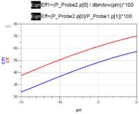
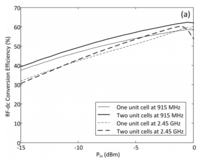
My simulation setup (fig1) and the corresponding results (fig2) are attached. I have also attached the schematic (fig3) and the corresponding result (fig4) shown in the above mentioned paper:

fig1 to 4:


I have couple of questions:

(a) Since I am doing the rectifier simulation first time (after reading many threads on edaboard), please tell me if my way to simulate the circuit (that is, the simulation setup) for efficiency is correct or not.

(b) As discussed in the above thread, I have defined the efficiency in two ways: eff and eff1. How these two parameters differ? I think "eff1" should be the correct measure of efficiency as it measures efficiency with respect to the input power. I think in "eff", the reflected power is not being considered. I am not sure, please suggest correct way to define efficiency in context of RF rectifiers.

(c) Neither eff nor eff1 matches exactly with the result shown in the paper (fig4, I am considering two unit cells at 915MHz). Why is this happening? I am considering the same diodes and have taken their model parameters from the datasheet (I guess the authors have taken it from the same datasheet- perhaps the only resource available online).


Thanks in advance for your precious time.

Note: I have asked this question at other forum but couldn't get any response.
 

(a) Since I am doing the rectifier simulation first time (after reading many threads on edaboard), please tell me if my way to simulate the circuit (that is, the simulation setup) for efficiency is correct or not.
I think there is no serious mistake in your simulation setup.

(b) As discussed in the above thread, I have defined the efficiency in two ways: eff and eff1. How these two parameters differ?
eff1 is similar to a transducer gain or |s21|*|s21|.
Its denominator is an available power of input signal source.

I think in "eff", the reflected power is not being considered.
"eff" is an ideal maximum efficieny.

I think "eff1" should be the correct measure of efficiency as it measures efficiency with respect to the input power.
It depends on purpose.

(c) Neither eff nor eff1 matches exactly with the result shown in the paper
(fig4, I am considering two unit cells at 915MHz).
Why is this happening?
Show us S11 as results of LSSP.

Increase Order[1] of both HB and LSSP, for example, 15 or 31.

Surely read https://www.edaboard.com/threads/354542/
Show us Eff2=( P_probe2.p[0] / sum(P_probe1.p) )*100.
 
Last edited:
Thanks a lot for your response.

Here are the simulation results with the increased order[1]=15:
fig5: Simulation setup
fig5.PNG
fig6: Simulated results
fig6.PNG
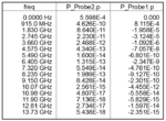
Also, I have probe results in a tabular form as follows with pin=0dbm (not sure if you wanted them in this format)
Table1: Probes results
Table1.PNG

Please note that in the above setup, I have set "pin" as a sweep variable in HB1 only.

If I set "pin" as sweep variable in HB1 as well as in HB2, then I get error as in the following figures:
fig7: Simulation setup
fig7.PNG
fig8: Simulation results
fig8.PNG

And one more thing that I get a warning simulating this circuit in each case:
fig9: warning given by ADS
fig9.PNG

It thinks this warning is just about ADS taking care of convergence issues.

With reference to your reply distinguishing eff and eff1, kindly also explain me with example what do mean by "It depends on purpose." . Because, I am unable to think why would someone be interested in eff when eff1 is the actual overall (simulated) efficiency that is achieved .
 

And one more thing that I get a warning simulating this circuit in each case:
fig9: warning given by ADS
View attachment 135323

Try putting a low ohm resistor inline with C9 and/or C10. I get the 'singular matrix' error when I have two series capacitors connected directly to supply rails. I suppose the simulator is unable to calculate an RC time constant. It cannot reach convergence.
 

Try putting a low ohm resistor inline with C9 and/or C10.
I get the 'singular matrix' error when I have two series capacitors connected directly to supply rails.
I suppose the simulator is unable to calculate an RC time constant.
It cannot reach convergence.
Wrong.
C9 and C10 constitite paralell connection to ground.
They don't cause any problem in simulation.

And one more thing that I get a warning simulating this circuit in each case:
fig9: warning given by ADS
.................................
It thinks this warning is just about ADS taking care of convergence issues.
L9 and L5 constitute inductive loop.

I think L9 and L10 are RF choke for DC bias setting for Diode.
You can delete L9.
However you can not delete L10.

Set small R for both L9 and L10.
 

Thanks, again, BradtheRad and pancho_hideboo. I added very small resistors (=0.01ohm) in series with L9 and L10 and the error messages disappeared.

Re-simulation with the modified settings doesn't change the results as L9/L10 are for providing DC path to ground for the rectified DC. I understand that L5 can perform this function in lieu of L9, that's why you said L9 can be removed.

In my above reply, why are the P_Probe1.p readings in Table1 negative at the 2nd harmonic onward? That perhaps causes efficiency with "sum(P_probe1.p) " to be different (more) from that with just P_probe1.p[1]? What about the other results, do they make sense?
 

I denote efficiency of "Two unit cells at 915MHz" in Fig.4 as Eff0.

Eff0 is located between Eff1 and Eff.
For small input level, Eff0 is close to Eff.
For large input level, Eff0 is close to Eff1.

Here are the simulation results with the increased order[1]=15:
Increase order[1]=31, then show Eff2.

Your S(1,1) in Fig.6 is completely meaningless.

If I set "pin" as sweep variable in HB1 as well as in HB2,
then I get error as in the following figures:
You have to specify full name for pin.
You have to understand data structure of "*.ds" file.

Show me S(1,1) as a result of LSSP with power sweep.

With reference to your reply distinguishing eff and eff1,
kindly also explain me with example what do mean by "It depends on purpose.".
Surely consider relations of Eff0, Eff, Eff1 and Eff2.


I understand that L5 can perform this function in lieu of L9,
that's why you said L9 can be removed.
Correct.

In my above reply, why are the P_Probe1.p readings in Table1 negative at the 2nd harmonic onward?
Show me S(1,1) or Zin of all harmonics as a result of LSSP with power sweep.
 

Thanks for you help and precious time, Sir. Sorry for delayed response, I had a deadline.

In the setup shown in fig7 above , I have made the following changes:

(a) Pin is now swept from -35 to 10 dBm, both in HB1 as well as in HB2.
(b) The order is changed to 31, both in HB1 as well as in HB2.

The modified setup look like as follows-

fig10: the modified setup
fig10.PNG
and the simulation results are as follows-

fig11: simulation results for the setup shown in fig10
fig11.PNG

By properly reading the .ds, hopefully I understand how to call 'pin' in equation and I am not getting the erro as I had in fig8.

What impression I draw from fig11 is that the a decent matching occurs after the breakdown of the diode for pin around 5 dBm. If somehow i could establish matching below 0 dBm; eff and eff1 would get closer. Am I correct?

Also, please pardon my little knowledge of ADS, but I don't know how to get "S(1,1) or Zin of all harmonics as a result of LSSP with power sweep." I think i can do this at specific input power. For example, when I fix pin=0dBm, I can have the following table-

Table2: S11 (dB/degrees) vs index at pin=0dBm
Table2.PNG

Is this table what you wanted me to show? If not , please guide me how to give you the data you shought in the previous message.
 

If somehow i could establish matching below 0 dBm; eff and eff1 would get closer.
Am I correct?
Probably, correct.
Eff is almost unchanged.
Eff1 will be close to Eff.

Also, please pardon my little knowledge of ADS, but I don't know how to get "S(1,1) or Zin of all harmonics as a result of LSSP with power sweep.
Insert list of what(S(1,1)) in data display.
And show results.
https://edadocs.software.keysight.com/pages/viewpage.action?pageId=5928753
 
Last edited:

Thanks for bearing with me and helping me out.

And again, pardon my little knowledge, but i tried to figure out what you would mean by plotting what(S11).
As per the link you shared, "what()" just gives you the size and type of data, but I am sure you wouldn't be interested in that or are you:
fig12.PNG

So kindly clarify a bit more what do you want me to plot?
 

Well, even in the list format I am getting the same information- the data type and size.

I am attaching the workspace so that you can point out my mistakes. Thanks.
 

Attachments

  • EH_Edaboard_wrk.zip
    5.9 MB · Views: 229

You may download in the ADS2015 7zads file format from here:

**broken link removed**
 

I don't open zip file.
Zipping attachments is the required method to send files in formats not natively supported for upload in Edaboard. I don't understand what's your problem with zip files. Zip file content will be virus checked and never executed without explicit user confirmation on a computer with reasonable security settings.

You may download in the ADS2015 7zads file format from here
That's only o.k. because you uploaded the zip file before.
 

I have, perhaps one last question in this thread, about the grounded inductor before the diodes, Ldc. I read somewhere that this inductor provides dc path to ground. If i don't use Ldc then the return dc current would flow into the source impedance and efficiency would effectively get reduced.

I see the rectfied dc voltage is at cathode side of the diode, at the anode side there is no rectified voltage. I am unable to understand why one earth the dc current will have a return path, it just travel in one direction, doesn't it? And, do I always need to provided the dc path in rectifier?
How do I decide the value of Ldc?
 

Status
Not open for further replies.

Part and Inventory Search

Welcome to EDABoard.com

Sponsor

Back
Top