Continue to Site

Welcome to EDAboard.com

Welcome to our site! EDAboard.com is an international Electronics Discussion Forum focused on EDA software, circuits, schematics, books, theory, papers, asic, pld, 8051, DSP, Network, RF, Analog Design, PCB, Service Manuals... and a whole lot more! To participate you need to register. Registration is free. Click here to register now.

[SOLVED] quartus pin assignments problem

Status
Not open for further replies.

dipin

Full Member level 4
Full Member level 4
Joined
Jul 16, 2014
Messages
223
Helped
14
Reputation
28
Reaction score
14
Trophy points
18
Activity points
1,731
hi,
i am using quartus to connect a DAC daughter board to de0 nano soc through LTC connector. i am using i2c protocol.but when i do the pin assignments , its saying that ""value entered is not a valid location" .

i am trying to connect i2c_sda to PIN_A21 & i2c_scl to PIN_B21 in pin planner

my module initiation is
Code:
module fpga_i2c(

input clk,
input reset,
input i2c_select,
output reg i2c_sda,
output wire i2c_scl

);

this is the pin assignment table from manaual Capture.PNG
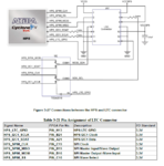
anybody know why this comming...if its not possible how can i connect it..


thanks and regards
 

Are you sure the pins are named PIN_A21 and not just A21? I don't have Quartus installed anywhere so I can't check.
 

are you sure that you select the device correctly ? "assignment > device "
if you've done anything correct in pin planner list of your inputs and outputs will be displayed and you can assign a pin for each from combo box
 

Are you sure the pins are named PIN_A21 and not just A21? I don't have Quartus installed anywhere so I can't check.

thanks for the replay ads-ee,

yes its PIN_A21..

please find the attached image of pin plannaer....i am able to assign to two pins(clock & one slide switch)....but not to pins related to LTC connector...Capture2.PNG

thanks

- - - Updated - - -

are you sure that you select the device correctly ? "assignment > device "
if you've done anything correct in pin planner list of your inputs and outputs will be displayed and you can assign a pin for each from combo box


yes hamidmoallemi, i am using de0_nan0_soc & you can see it in above pin planner image


Altera Cyclone® V SE 5CSEMA4U23C6N device

thanks

in de0_nano_soc user manual, LTC section is in page 41. iam using i2c interface for it
 

Reviewing Cyclone V manuals might help.

A21 is a dedicated SoC resource, it can't be used as FPGA fabric I/O. For the same reason, the pin isn't offered in the Pin Planner selection when assigning I/O signals.
 
  • Like
Reactions: dipin

    dipin

    Points: 2
    Helpful Answer Positive Rating
Reviewing Cyclone V manuals might help.

A21 is a dedicated SoC resource, it can't be used as FPGA fabric I/O. For the same reason, the pin isn't offered in the Pin Planner selection when assigning I/O signals.

thanks for the replay FvM,

but for communication to a DAC through LTC connector, by I2C protocol, HPS_I2C1_SCLK &HPS_I2C1_SDAT are the pins right?? ie PIN_A21 & PIN_B21..
if it not posssible to connect through it, any other way to send data through the ltc connector using i2c?

regards
 

You didn't tell what you want to achieve, but apparently the development board design expects that the I2C is controlled by ARM processor.
 

Use assignment editor rather than pin planner, or check the .qsf file to see if there is another variable handling these pins. You are perhaps using as template a design not 'empty', so something is likely already assigned to those pins as they said above.
 

You didn't tell what you want to achieve, but apparently the development board design expects that the I2C is controlled by ARM processor.

Hi,

i wanted to connect a dac daughter board to de0 nano soc through LTC connector using i2c interface. after that need to send a 32 bit data(as specified in 2607 manual) to dac and read the voltage on output.i am using LTC 2607 as daughter board.

thanks and regards
 

Hi,

i wanted to connect a dac daughter board to de0 nano soc through LTC connector using i2c interface. after that need to send a 32 bit data(as specified in 2607 manual) to dac and read the voltage on output.i am using LTC 2607 as daughter board.

thanks and regards
I'm not sure if you understand the SoC FPGA concept. The Hard Processor System (HPS) has a number of dedicated I/O pins that can't be directly accessed by the programmable FPGA logic. A21 is one of it. It can be only used as I2C pin by the hardware I2C controller in the ARM processor and respective C code. The pin could be also configure as ARM GPIO, but that doesn't help for your intention to address the pin from FPGA logic.
 
I'm not sure if you understand the SoC FPGA concept. The Hard Processor System (HPS) has a number of dedicated I/O pins that can't be directly accessed by the programmable FPGA logic. A21 is one of it. It can be only used as I2C pin by the hardware I2C controller in the ARM processor and respective C code. The pin could be also configure as ARM GPIO, but that doesn't help for your intention to address the pin from FPGA logic.

thanks for the replay FvM,

if it not possible to access the pins, then how can i do it. i dont have much idea about it ( i thought like i can access it directly)... can you or anyone give some hints to do it.

regards
 

if it not possible to access the pins, then how can i do it.
The only turn around option that I see worthy of an attempt is by disabling these 2 pins ( for example, defining them as input ) and connect other 2 pins externally, that you can manage. I do not know anything of the De0 nano board you are using, but usually in developmental kits many pins are available in general purpose connectors. Certainly this will imply in an undesired load effect as well will limit speed, but only testing to know in practice if it works or not.
 
  • Like
Reactions: dipin

    dipin

    Points: 2
    Helpful Answer Positive Rating
Status
Not open for further replies.

Part and Inventory Search

Welcome to EDABoard.com

Sponsor

Back
Top