Continue to Site

Welcome to EDAboard.com

Welcome to our site! EDAboard.com is an international Electronics Discussion Forum focused on EDA software, circuits, schematics, books, theory, papers, asic, pld, 8051, DSP, Network, RF, Analog Design, PCB, Service Manuals... and a whole lot more! To participate you need to register. Registration is free. Click here to register now.

Top level floor planning in ASIC physical design

Status
Not open for further replies.

preethi19

Full Member level 5
Full Member level 5
Joined
Jun 30, 2014
Messages
273
Helped
0
Reputation
0
Reaction score
1
Trophy points
16
Activity points
3,474
Hi i did a project in digital design and i had blocks like JTAG, control unit, buffer, clock generator, Tx unit. So i did the layout of the design using Cadence Encounter. Placement of cells were fully automatic. I didn't manually place the blocks. I understand what the term "top-level floorplanning" is and how for an efficient layout with consumed space, timing, power are considered while deciding how to place the blocks within the IC core. But i have no idea abt wat are the factors that needs to be considered and how to choose to place each block in an efficient manner. Can anyone pls give me a good link or pls list out the main factors that are always considered while doing top-level floorplanning. Pls help!!! Thank you!!! :)
 

either minimise the cutset of the nets between blocks or meet the timing constraint.
 

Manual placement of individual digital blocks in IC core layout

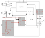
Hi pls have a look at the attached image.
digital layout.png
It is a digital design and the layout of this design using Cadence Encounter is completely automatic placement of the digital blocks. I am learning about manual floor planning. Problem with automatic placement is that you don't get to decide in what order the digital blocks needs to be placed. Suppose say (just for eg) i want to place the JTAG below the TX unit. Can anyone pls tell me how i can manually do that? Meaning when i give the place option in Encounter it places the entire design with so many blocks (ie) the JTAG itself is comprised of so many individual blocks and since its layout i am not able to find which blocks belong to JTAG and which are of say TX unit and so i am not able to select the entire JTAG unit and place it under the TX unit and do the routing. I am totally new to manual placement so i have not much clue so kindly bear with my questions! Can anyone pls explain to me. Thanks a lot! :)
 
Last edited by a moderator:

Thank you for the reply! So top level floor planning can be done in any way as long as timing constraints are met? Are there anything else other than minimising cut set while doing top level Floor planning? I understand about cutsets and also about minimal cut sets. But when an ASIC has millions of logical elements how is it manually possible to say remove some components of the cut-set bringing it down to a minimal cut set? Is there any method for that?
 

we dont talk at logical elements level.
we consider only the module level.
the modules have certain nets.(coming out and going in).

it is not removing some components.
it is about the arrangements.
 
Oh ok i get it now. I was looking in terms of logical level. So then if its about modules and about the nets (that go in and out of them), can you kindly pls let me know what you meant by "minimizing cut sets". Becoz if certain no of nets connect from one module to another how can we minimize the net connections? or is just like the way you told we just retain of the nets but the method of arrangement would vary. Am i getting it right? Like i want to understand based on what factors do we decide on the arrangement. For eg i found this that for floorplanning we "Keep the highly connected blocks physically close to each other." So like this wat are the other things that we need to be looking. Kindly let me know! Thanks for the replies so far :)
 

As you said ,
just retain of the nets but the method of arrangement would vary. ...
"Keep the highly connected blocks physically close to each other." ...

keeping the highly connected nets close to each other is the major cost you can consider and play (move) with the modules.

So identifying 'highly connected modules together ' is the task in placement.
 
As you said ,


keeping the highly connected nets close to each other is the major cost you can consider and play (move) with the modules.

So identifying 'highly connected modules together ' is the task in placement.

Not placement, floorplanning.

There is much much more to consider than simple nets. You have to think of channels between modules, proximity between critical parts, critical IO, buses, and so on. You might want to put some hard IP close together but you can't because it becomes too deep. So you start to interlace std cell area with IP area. You come up with donut-shaped arrangements. You also have to think of power islands, blocks that shut down together will usually stay together. You also have to think of power grids and how to deliver power to all the crazy looking modules sitting in all sorts of different places. You also have to think of your IO ring and how it limits/enables your design.

There is a reason why companies have their senior engineers doing top level floorplan. It's because it is damn hard to optimize all of these at the same time.
 
Thanks a lot for the reply! I understood well about the issues of floorplanning. Could anyone also kindly take a look at the part of 'Manual placement of individual digital blocks in IC core layout" in this post above and help me with it please. I have attached an image along with the query. :)
 

Status
Not open for further replies.

Part and Inventory Search

Welcome to EDABoard.com

Sponsor

Back
Top