Continue to Site

Welcome to EDAboard.com

Welcome to our site! EDAboard.com is an international Electronics Discussion Forum focused on EDA software, circuits, schematics, books, theory, papers, asic, pld, 8051, DSP, Network, RF, Analog Design, PCB, Service Manuals... and a whole lot more! To participate you need to register. Registration is free. Click here to register now.

applying T network in hfss

Status
Not open for further replies.

prateek3790

Full Member level 2
Full Member level 2
Joined
Feb 8, 2016
Messages
131
Helped
1
Reputation
2
Reaction score
1
Trophy points
18
Activity points
1,190
hiiii
i am using a lumped T network in HFSS now i have to place this between two microstrip lines. s1 and s2 are the series arm of the T network and p3 is the parallel arm of the T network then how i am supposed to connect this to the two tr line. i connected s1 and s3 to the conductor of the microstrip lines and (by keeping two sheets and giving them rlc boundary of their specific values ) and the parallel arm is connected to the ground of the microstrip line on one end and on the common edge of these series arm on the other end.
is this the correct way to implement this
 

If you included a picture and described your BCs, it might be easier to double check your work. From what you described, it sounds like you are on the right track making 2D structures and assigning lumped element RLC boundary conditions. It is correct to connect the series ends of the T to the core conductors of the microstrips and the parallel portion of the T to the ground conductors of both microstrips.
 

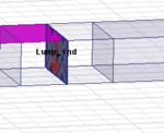
see i applied a L network . capacitor is connected directly to the conductor of microstrip and the parallel inductor is connected to common ground of the microstrip line and one side i increased the conductor of microstrip line so that inductor can be separated from the surface of substrate.
is this correct.
 

Attachments

  • cap_boundary.PNG
    cap_boundary.PNG
    10.4 KB · Views: 122
  • Common_ground.PNG
    Common_ground.PNG
    29.9 KB · Views: 124
  • tr1.PNG
    tr1.PNG
    8.9 KB · Views: 119
  • tr2.PNG
    tr2.PNG
    8.3 KB · Views: 129

If the top rectangular face is a separate conductor from the bottom rectangular face and the space in between is your substrate like you say, then yes I believe that is correct. You should have two transmission lines connected by a shunt inductor and series capacitor. Are there any oddities in your results that would make you think something is acting up?
 

actually after using this matching network it was supposed to be matched to 50 ohm but (for certain value of l and c) but when i used those value in hfss simulation it is tuned to frequency other than what i used to calculate.(2.4 ghz- analytical resonant frequency 2.2 ghz- simulated resonant frequency ).why is that ?
 

Status
Not open for further replies.

Similar threads

Part and Inventory Search

Welcome to EDABoard.com

Sponsor

Back
Top