Continue to Site

Welcome to EDAboard.com

Welcome to our site! EDAboard.com is an international Electronics Discussion Forum focused on EDA software, circuits, schematics, books, theory, papers, asic, pld, 8051, DSP, Network, RF, Analog Design, PCB, Service Manuals... and a whole lot more! To participate you need to register. Registration is free. Click here to register now.

Adaptation of a 50Ω Port to a CMOS Ring Oscillator in AWR AO

Status
Not open for further replies.

cannibol_90

Member level 5
Member level 5
Joined
Jun 20, 2009
Messages
83
Helped
5
Reputation
10
Reaction score
5
Trophy points
1,288
Visit site
Activity points
2,066
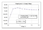
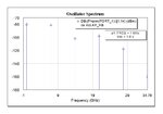
Now, we are getting a linear output for the CS-VCO from 1GHz to 5GHz. This is when we attached M_Probe (Measurement Probe) to view the output voltage with respect to time. But, attaching a 50 Ohm port collapses the output because of the impedance mismatch? From what we have seen, a 50 Ohm port pulls current (in mA) into it. To nullify this current, we had to increase the port impedance to as high as 100 Mega Ohm to 1 Giga Ohm. We need a 50 Ohm port to check for Oscillator noise, Tuning Range, Output power spectrum etc. As 1 GOhm is impractical for real life scenario, what are we doing wrong? Or are the parameters to be blamed for? Or, is any matching circuit needed here?
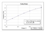
linear.jpg
spectrum.jpg
power.jpg
 

Hi,

Our problem is with the adaptation of a 50Ohm port to a MOSFET circuit. For example, when we constructed a basic CMOS inverter, a proper output COULD NOT be observed with an output port of 50Ohm impedance. But, when we increased the port impedance to be very high like 1GOhm, a proper output was observed. What could be the reason behind this problem? How can I measure the output with a 50Ohm port impedance?
 

The RO may have two problems. One is weak output drive.
The other is that loading its output kicks that current into
the supply / ground rails where it can destabilize, mode-
shift or quench the oscillation.

I recommend using a resistor divider network to get a
scaled, 50-ohm output (like, 4950 series and 100 ohms
to VDD and VSS in shunt). Sure, you're now looking at
10mV rather than 1V, but at least it ought to be clean.

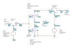
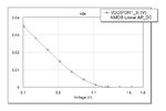
Yes! Indeed, the output is being pulled to the ground at lower terminating impedances. The below circuit shows that the output port draws some current into it at 50 Ohms with very less voltage at the output node, but 0A at 10 GOhms.

CMOS Inverter with a termination of 50 Ohms.
50 ohm termination.jpg
CMOS Inverter output at 50 Ohm termination.jpg

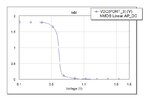
CMOS Inverter with a termination of 10 GOhm termination.
10 GOhm termination.jpg
CMOS Inverter output at 10 GOhm termination.jpg

Can MOSFET be used in some configuration to match the output to 50 Ohms? Is it a impedance matching problem?
 
Last edited:

Can MOSFET be used in some configuration to match the output to 50 Ohms? Is it a impedance matching problem?

Your mosfets are turning on sufficiently to create voltage swings on a high impedance load.

You need to turn on your mosfets to a greater extent, meaning their On-resistance needs to go lower. Then they can drive a low impedance load.

It's possible they need greater Off-resistance as well, to create useful voltage swings.

I do not know specifically how you might achieve this in a ring oscillator. It might have to do with the capacitance of the mosfet gates. Etc.
 
A ring oscillator is typically made with near-minimum sized
devices and can't be expected to drive a significant load.
In the interest of highest attainable frequency, its taper
factor is 1:1. You can't get to a normal off-chip drive
strength without a tapered buffer (typ 4:1 and multiple
stages) which would unfortunately ruin bandwidth relative
to the RO core (and then also chew mucho power with those
stages operating in "valve float" full time).

Did you try the idea of a high Z in, 50 ohm out attenuator
network in your simulator?

If this RO is totally unbuffered then the loading problem
may be more severe than just amplitude; with too few
gain stages, you could de-Q the ring enough that it can't
even sustain oscillation at the frequency of interest.
Hopefully there is at least 1-2 stages of 1:1 taper buffer
so that loading can't affect the oscillator core itself, and
then you have only the drive / amplitude, and self-noise
loading issues to deal with.
 
Your mosfets are turning on sufficiently to create voltage swings on a high impedance load.

You need to turn on your mosfets to a greater extent, meaning their On-resistance needs to go lower. Then they can drive a low impedance load.

But, we are using TSMC 180 nm model parameters for the MOSFET model. And the maximum allowed voltage is 1.8 V, right? We are not allowed to change Cox et al..
 

Your circuit has some output impedance which produces maximum power in a load. By experiment you can find the load resistance. It might be 500 ohms, or 50 k, or 5M. It will draw some midway voltage, at some midway Amperes. The goal is to get maximum Watts.

Once you find out what this impedance is, you might contrive a transformer, or, an LC 2nd order filter arrangement, to match it to a 50 ohm impedance. It may result in a different voltage, and different Ampere level. Nevertheless it should be measurable.

I believe this is similar to the idea mentioned in post #6 ('high Z in, 50 ohm out attenuator network').
 
In the AWR example of Ring Oscillator schematic shown below, there is no 50 Ohm port attached. Instead a series capacitor is used.

RO.jpg

1. In AWR simulation, a 50 Ohm port is used for the measurement of phase noise, output power, oscillation frequency and so on. Is that the case during measurement in Analog ICs? How are measurements performed in Analog ICs? What is a high Zin 50 Ohm port? Is this used for measurement in Analog ICs?

2. In the schematic shown above, there are two contact resistors used namely nwell and substrate contact. What are the use/significance of these resistors? Why can't we directly short the Body and Source terminals to avoid Body Effect?

3. We have been instructed to use VSS instead of ground in our circuit. Why can't Analog circuits be directly connected to ground? Are VSS and ground one and the same? What is the difference?
 

There is no "high Z 50 ohm port". 50 ohms is a near
universal standard (75 for cable TV). You have to
impedance-transform between your source and your
load, sometimes (or nearly always, in modern low
voltage RF wanting any power at all - voltage being
fundamentally process-limited, current being a matter
of how much area you're willing to spend, impedance
falling out of that choice at the driver end but not
moving one bit at the antenna or PCB end).

Your NWell and substrate contacts are indeed resistive
and the resistors may be for noise-effects accuracy,
if they are ohm-range values. If they are trivial (like 10m)
then perhaps they are to prevent netlisting errors about
shorted global nets. You'd have to dope out the schematic
to netlist scheme, to say.

You can do all kinds of unrealistic things in schematic land
that aren't analog-realistic. Such as declaring that your
chip ground is zero-impedance-equal to your prime
reference (measurement equipment) ground. Honesty
demands you represent the real connection. Freedom
to represent, requires multiple "zero volt" domains (so
you may see vss!, vssa!, vssd!, gnd!, gnda!, gndd!, ...).
 
Your circuit has some output impedance which produces maximum power in a load. By experiment you can find the load resistance. It might be 500 ohms, or 50 k, or 5M. It will draw some midway voltage, at some midway Amperes. The goal is to get maximum Watts.

Once you find out what this impedance is, you might contrive a transformer, or, an LC 2nd order filter arrangement, to match it to a 50 ohm impedance. It may result in a different voltage, and different Ampere level. Nevertheless it should be measurable.

I believe this is similar to the idea mentioned in post #6 ('high Z in, 50 ohm out attenuator network').

As per your advise, we measured the output impedance for maximum power transfer. An output impedance of 20KOhm was observed for a control voltage of 0.5V and 11KOhm for 1.1V. But these are for an oscillation frequency of 1GHz and 6GHz respectively. How to impedance match for this entire range of frequency?

VCO 1.1V 11KOhm.jpg
VCO 0.5V 20KOhm.jpg
 

I'm not sure you -want- maximum power transfer. If the RO
is unbuffered then maximum power out, means minimum Q
in the core loop. Even if buffered, the more power you extract
the more you perturb the supply rails.

My belief is, if you are only interested in frequency then you
either want to measure with as little power taken as possible,
or you want to take the same power as the end application
would. We don't know the latter. The former, you have to
trade between noise floor (phase noise measurement
quality) and power-take-induced perturbation of the RO's
operation. I'd say to creep up on it from minimum and see
where things get acceptably repeatable and sane.

Many modern impedance matching / transforming methods
are narrowband and can't give you 50 ohms across wide
frequency ranges. Even the resistor divider I had proposed,
has issues of high frequency rolloff is presented any shunt
C (hopefully, your shunt is 50 ohms resistive and low enough
L in the interconnections not to matter - at 6GHz, though,
good luck.
 
**broken link removed**

This is an example of Ring VCO from Agilent. It is seen the output of each inverter uses load capacitor. What is the use of this load capacitor?


ring vco.jpg
 

One desirable attribute of a current starved ring oscillator
is consistency of frequency vs voltage & temperature. The
MOS caps add to the phase shift per stage (C/I) with the
least temperature-variable characteristic of the available
devices (small FETs' D-B capacitance being very temp and
supply variable, while a well-inverted MOS cap is mostly
just Cox, invariant with all except process). You take a lower
max frequency for more well behaved frequency.

This picture is indeed an unbuffered ring oscillator and any
loading of the output must be expected to perturb the
operation. It seems to be the norm, that ROs are on-chip
divided which really eases the parasitics issue as well as
naturally buffering the oscillator core from external
influences.
 
Few questions...

1. Without the 50 Ohm port, how do we measure the TOTAL power consumption (AWR needs a port to measure some of the parameters)? At the maximum power transfer, is it the correct method to sum the power consumed by all MOSFETs and other devices? If not, how to calculate the net power consumed?

2. Is there any problem with the aspect ratios (W/L) of the MOSFETs being 1?

3. As there is a feedback, will buffering lead to a degradation in output?

- - - Updated - - -

4. Can correct aspect ratio and buffering lead to a proper output match?
 
Last edited:

Status
Not open for further replies.

Similar threads

Part and Inventory Search

Welcome to EDABoard.com

Sponsor

Back
Top