Continue to Site

Welcome to EDAboard.com

Welcome to our site! EDAboard.com is an international Electronics Discussion Forum focused on EDA software, circuits, schematics, books, theory, papers, asic, pld, 8051, DSP, Network, RF, Analog Design, PCB, Service Manuals... and a whole lot more! To participate you need to register. Registration is free. Click here to register now.

Implementing a virtual ground circuit design for large current

Status
Not open for further replies.

T3STY

Full Member level 4
Full Member level 4
Joined
Apr 17, 2012
Messages
239
Helped
24
Reputation
48
Reaction score
24
Trophy points
1,308
Visit site
Activity points
3,715
I need to design a split power supply starting from a single power supply. The single power supply is supposed to be 24V (at least 2A) so as to have a perfect 12-0-12 split supply, but I'd like to be able to use even one as low as 19V (still 2A minimum).
The required output power of the split supply is at least 9V@1A each.

I have searched the web for designs and seems all of them have pros and cons. Next there are the two designs that convinced me the most.

The first one is based on a resistor voltage divider and a low power opamp integrated into a IC, the TLE2426; then a buffer opamp would sustain the large output current.
This circuit is capable of driving my output power needs, but by looking on various websites people say it can only support a certain amount of capacitance on the output (that specified by the opamp manufacturer), which should not be exceeded for proper operation.
The circuit has been originally found on tangentsoft.net (LINK)
rail_splitter_opamp.png

The second one is based on an unusual way of using linear voltage regulators. By wrapping two complementary voltage regulators (the famous LM317/337 or 7812/7912 ect.) into a voltage divider circuit, their regulation output will maintain a nice and stable voltage for each line. Their joint output becomes the VGND.
This design has been originally found on head-fi.org (LINK)
rail_splitter_VReg.png
EDIT: R1 and R2 should be chosen based on the input voltage and they should provide 1.5mA through the LM336 diode
While this circuit is pretty much perfect, it heats up. Like a lot. I am able to provide a large heatsink for the regulators, but I'd like to avoid it if possible. And also, it might hide caveats that the original designer has not considered to exist in first place.

I know I can count on smart people on this forum and I'd appreciate if you could tell me if one of these is the best solution to go with, or if there are any better alternatives, and even how to make better the designs that I have posted.
Thank you very much to any one who replies ;)
 
Last edited:

What circuit do you have that needs a low impedance virtual ground at 1A for each polarity?
Usually if the high impedance low current input of an amplifier is biased and filtered at half the supply voltage then its output will also be at half the supply voltage if it is capacitor coupled so that its DC gain is 1.
 

The circuit is to be used for a small portable bench test, with a prototyping breadboard on it. I actually don't care if the output is low or high impedance (I don't even know the difference to be honest) as long as I can use as many components as I want without worrying about reaching the current limit. I thought of 1A as a safe limit, but I hardly think I would reach 2A total. Just in case I would prototype some audio amplifier or something I might be going that hard on it, and that's why I thought 2A (1A+1A) would be some safe maximum limit. Actually, I am building this for a friend of mine as well who often does things with amplifiers and things that require a bit of power.

Suggestions are gladly accepted ;)
 

I show an opamp but it could be an audio power amplifier.
On the left side there are circuits with a positive and negative dual polarity supply. You are trying to make this from a single supply by using brute force to feed the power supply for the amplifiers.
On the right side I show amplifiers that have a single supply and are biased at half the supply voltage with two high value resistors. Brute force is not needed.
Both ways produce exactly the same outputs.
 

Attachments

  • opamps.gif
    opamps.gif
    16.8 KB · Views: 483

None of the circuits in post #1 is suitable for 1A virtual ground current.

I presume you understand that the virtual ground must be only sourced/sunk by the power supply and that the amplifier driving the ground node must be designed to handle the respective power disspation, e.g. 9W vor 9V*1A. Another option would be a bipolar switched mode power supply.

The first point would be to define if you want strict mid supply or a regulated voltage above negative rail (as in the first post #1 circuit). Secondly you'll specifiy besides current delievery the required impedance of the virtual ground node.

A straightforward solution would be an OP buffer followed by a push-pull common emitter transistor stage with overall feedback.
 

Let's make it clear: although this virtual ground power supply is going to be used for audio amplifier prototyping too, it is intended for a much more general use. As I said, it would be the power supply to use on breadboard prototyping, so I could even use it to power other ICs, including digital ICs like PICs and other MCUs (with a proper 5V or 3.3V voltage regulator, obviously).


The circuits posted by Audioguru are exactly the same as the first one that I posted. The TLE2426 includes a resistor voltage divider plus a buffer opamp (and probably some other stabilization circuitry). This IC will only make sure the input voltage is split in a perfect half (with maybe 0.1V error). However, the TLE2426 can only sink/source up to 40mA (or 80, can't remember), which is why the output goes into a high power buffer opamp that supports 1A or more current. The only caveat here is that the opamp should support high currents at unity gain.

FvM, you're grounding me :D
Yes I know about the amplifier power dissipation, but that's an afterwards thought. For now I am only trying to get the split power supply done for a much more general use.
Can you please elaborate a bit more about the strict mid supply or regulated voltage above negative rail? I also have no idea of what impedance it should have... I suppose, for a generic power supply, the lower the better?
And lastly, I found some websites that suggest using an opamp with a push-pull C.E. transistor on the output. Do you think this is a far better idea? If you could show an example of it, would be great.
 

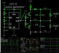
This is conceptually a voltage doubler, but it can provide an adjustable split supply as well.


The 555 cannot tolerate more than 18V. I used it because it is a convenient device to bias the transistors so that they never conduct simultaneously.

With light load the capacitors will each charge to 22V. Therefore you will need to vary the duty cycle to each transistor independently, to adjust output voltages.

- - - Updated - - -

Also notice the supply gets continual current taken from it. At no time does current draw go above your spec value of 2A. (Edit-I was incorrect. The supply does send more than 2A when loads draw 1A each.)
 

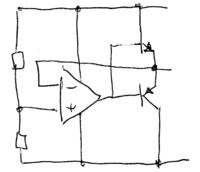
I wrote "common emitter", but I actually meaned common collector respectively voltage follower, as shown below.


Thank you guys. As soon as possible I will get some components and test the solutions you have suggested. I'll let you know if something is not working :)
 

Below is the LTspice simulation of a circuit similar to FvM's concept.
I added compound transistor stages to handle more than a 2A imbalance and some feedback compensation to avoid oscillations from the C1 and C2 filter capacitors in typical loads.

The virtual ground voltage is shown for a 2A plus and minus imbalance.
There is a small spike in the virtual ground voltage when the unbalance transitions from plus to minus but that is unlikely to occur during normal circuit operation with more or less fixed loads.

Note that there can be significant power dissipated in Q1 and Q4, equal to the imbalance current times 12V, which would be 24W for a 2A imbalance, so they will need to be on an appropriate heat sink.
 

Attachments

  • Virtual Gnd.gif
    Virtual Gnd.gif
    35 KB · Views: 467
Last edited:
  • Like
Reactions: FvM

    FvM

    Points: 2
    Helpful Answer Positive Rating
As expectable, the crossover of the class B buffer causes a delayed response with an output glitch. Also the bypass capacitor load enforces a compensation network to achieve stability.

If better performance is required, you'll use a relative fast OP (in terms of bandwidth and slew rate), not the slow LM324 with only 0.5 V/µs. But the basic circuit behaviour, including the stability problems with capacitive load, is the same.

Depending on the application, a non-feedback buffer with respective load dependend voltage drop may be a simple alternative.
 

As expectable, the crossover of the class B buffer causes a delayed response with an output glitch. Also the bypass capacitor load enforces a compensation network to achieve stability.

If better performance is required, you'll use a relative fast OP (in terms of bandwidth and slew rate), not the slow LM324 with only 0.5 V/µs. But the basic circuit behaviour, including the stability problems with capacitive load, is the same.
...............
Due to the reduced risetime from the feedback network, the slew rate of the LM324 is not the limiting factor in the crossover spike.
 

I was suggested of using two switching voltage regulator circuits (maybe based on the LM2596-ADJ like *this one*, or other ICs) on the splitted voltage lines. It would allow to regulate the output voltage on each line so I could achieve a different dual supply voltage (e.g. 9-0-9 or even 8-0-12 but I'm not sure I'll ever use asymmetric voltage).
Will this be of any trouble to the rail splitter?

@crutschow: about those little spikes of your circuit, will they still occur if I will use some switching voltage regulators afterwards? I suppose they won't happen at all if the load never switches from positive to negative voltage, but I'm no expert and I'd like to be sure of it.
 

You can use the rail splitter to get unequal voltages, if you want just by changing the relative value of R1 and R2.

The spikes only occur when the imbalance in current shifts from positive to negative between the plus and minus.
For steady loads you won't see them.

If you are going to the trouble of adding two switching regulators, then why not supply them with separate isolated voltages and you won't have to mess with a virtual ground circuit?
 

I think a problem of the thread is lack of a clear specification of the intended power supply, so the solutions are jumping around between low current circuits (initial post), high current virtual ground and finally switching regulators,

Whatever you want, combining a linear virtual ground circuit with a dual switching regulator doesn't seem to make much sense.
 

I need to use an external power supply, like a laptop power supply, to power up the entire project test bench project. I will need a digital power supply (both 3.3V and 5V) which I have already figured out how to achieve, and then I need a split power supply that should be achieved from a single supply like a 24V one. The rail splitter will just achieve this last step. I might need to adjust the split power supply voltage to something lower than the exact half of the input voltage and I thought I'd use switching voltage regulators on the rail splitter output lines.
I hope it is clearer now :)
 

I hope it is clearer now
As said, it doesn't look like a good design idea. I would feed a buck converter and an inverting buck-boost converter by the 24 V source to make a dual supply.
 

I appreciate the advice, FvM.
I have tried that path already but I am unable to design such circuit, they are too much out of range for my limited knowledge. You may remember I have asked about buck-boost converters a few months ago, you've been one of the users who helped me with that. You may also remember that an inverting buck configuration is heavily limited in the amount of output current (a few hundred mA, certainly not 1A) or at least, the designs we've considered were limited.
 

......................
that an inverting buck configuration is heavily limited in the amount of output current (a few hundred mA, certainly not 1A) or at least, the designs we've considered were limited.
Certainly there are numerous inverting buck converters that can deliver more than 1A, although they may require an external MOSFET for that current.
 

You may also remember that an inverting buck configuration is heavily limited in the amount of output current (a few hundred mA, certainly not 1A) or at least, the designs we've considered were limited.

The topology isn't limited of course. Your split supply + switched mode supply idea involves a negative buck converter for the neative rail. I could also argue that there are no suitable negative buck converters avaible.

Instead of starting with circuit topologies, you should start with a problem specification. Available input voltage, required output voltage(s) and current(s). There are always different ways to achieve it.

But this is a thread about supply splitters and we shouldn't turn it into a boundless discussion about power supply topologies. Edaboard users that are searching for answers should have a little chance to find it when looking at thread titles.

I just realized that a possible solution hasn't been mentioned yet. Using a synchronous buck converter with duty cycle of 0.5 as "lossless" switched mode supply splitter.
 

Status
Not open for further replies.

Similar threads

Part and Inventory Search

Welcome to EDABoard.com

Sponsor

Back
Top