Continue to Site

Welcome to EDAboard.com

Welcome to our site! EDAboard.com is an international Electronics Discussion Forum focused on EDA software, circuits, schematics, books, theory, papers, asic, pld, 8051, DSP, Network, RF, Analog Design, PCB, Service Manuals... and a whole lot more! To participate you need to register. Registration is free. Click here to register now.

Darlington based GDT driver

Status
Not open for further replies.

boylesg

Advanced Member level 4
Joined
Jul 15, 2012
Messages
1,023
Helped
5
Reputation
10
Reaction score
6
Trophy points
1,318
Location
Epping, Victoria, Australia
Activity points
11,697
I am having trouble using a pdip UCC27425 to drive a GDT - presumably the chips don't have enough power to drive my GDT and I keep blowing them rather spectacularly I might say.

I am trying to implement the same functionality using TIP120, TIP125, HEF4069UBP and HEF4081B.

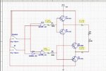
Here is my design:
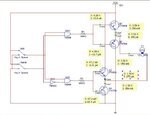
GateDriver.jpg

When testing my actual circuit I am getting a short when the two logic inputs 555 and Aerial are at 12V. I blew a fuse.

I checked my circuit for any obvious soldering mistakes and bridges etc and can't see any.

Are there any obvious design flaws that anyone can spot?
 

What is a "GDT"?? Your simulator thinks it is a 12V/25W incandescent light bulb.

You should not destroy an old 74xx TTL logic input with nearly +12V input. Their maximum allowed input voltage is only +5.5V.
Their maximum output voltage is only about +2.4V to +3.6V so they are useless in that circuit. The light bulb might get a volt or two if you are lucky.
 

Change R1,2 to 0 ohm jumpers.

OK thanks, but why don't you need any resistors on the outputs of the logic gates?

What would limit the current?

I was aiming to limit the current on the base of the darlingtons to 20mA which means they would be in saturation.

- - - Updated - - -

What is a "GDT"?? Your simulator thinks it is a 12V/25W incandescent light bulb.

You should not destroy an old 74xx TTL logic input with nearly +12V input. Their maximum allowed input voltage is only +5.5V.
Their maximum output voltage is only about +2.4V to +3.6V so they are useless in that circuit. The light bulb might get a volt or two if you are lucky.

GDT = Gate Drive Transformer - 1 primary and 2 secondaries to drive a FET half bridge. Ratio 1:2:2

I have been using an automotive light bulb just to make sure that I have the logic correct, in which case I can see a result rather than having to measure with my multimeter.

Previously I was using a gate drive IC - UCC27425. Dual gate drive, one inverting and one non-inverting. The GDT was connected across the two output pins via a 680nF cap. But with a 555 running at about 20kHz on the enable pins and another 555 running at about 80kHz (simulating the noise spikes from a tesla coil coming in from an aerial through two series schmitt trigger hex inverters), my UCC27425 was running very hot and kept blowing up...literally.

So despite the supposed 4A transient max output from these chips specified in the datasheet, they are apparently not good enough to drive my GDT or else I am doing something else wrong with them that I don't understand.

I built a plasma globe driver based on a similar single darlington totem pole driving the GDT primary from GND rather than another totem pole. This proved to be very robust but now I am trying to replicate the functionality of the UC27425 with two darlington totem poles.
 

The logic high output voltage from a very old 7408 TTL logic IC is much too low for your circuit where the darlington emitter-followers reduce the output voltage even more. It also has much too low current to saturate your darlingtons. The datasheet for the 7408 shows an output high of only 2.4V to 3.6V at a maximum of only 0.8mA.
 

The logic high output voltage from a very old 7408 TTL logic IC is much too low for your circuit where the darlington emitter-followers reduce the output voltage even more. It also has much too low current to saturate your darlingtons. The datasheet for the 7408 shows an output high of only 2.4V to 3.6V at a maximum of only 0.8mA.

Audioguru, I am not actually using those 74 series logic gates depicted in the circuit.

I am actually using HEF series where the logic high voltage is 14.95V for a 15V supply.

When constructing that circuit in the simulator I only have the 74 series available to me.

I tried to find a spice model for the HEF but NXP does not seem to have any models at all available for download on their website.

So the best I can do with that simulated circuit is to test that I have the logic right if not the resistor values and saturation etc.

I suppose for the latter I will just have to manually set all the possible logic combinations with a direct connection to the battery terminals and then measure the current flowing into the bases of my darlingtons with my multimeter to find the right resistor values.

From my inaccurate simulated circuit it appears that the resistor values for the NPN and PNPs may need to be different, assuming the 74 series behaves roughly similar to the HEF series.

I have added some 1.5k resistors on all the inputs of my real HEF inputs to limit the input current to less than 10mA. With them in place my HEFs are no longer running hot.

I also need to make sure that there is no chance that any of my logic inputs are floating because that messes things up as well, creating short in my totem poles. I didn't think of that originally. I probably should put a 100k resistor to GND on all my inputs, particularly while I am testing with direct battery terminal connections.

When my real circuit is connected up properly my 'enable' input will be connected to the output of a 555 so that it will always have a definite state.

But the 'in' pin may be connected to an aerial input that may or may not have the aerial attached. This input has a diode clamp:
broken link removed

And I am assuming that this would still be regarded as a floating input. Is that correct?

- - - Updated - - -

P.S. If you have or know where to get SPICE models for the HEF series or equivalent logic ICs then I would greatly appreciate you pointing me in their direction.

It would be rather useful to be able to simulate my circuit more accurately.

According to the TIP 120/125 datasheets, the max 10mA output of the HEF4081BP is enough to saturate the TIPs. But I guess I could always bump it up a little more by means of some BC547s and BC557s.

But I can't simulate this unless I can find some SPICE models of the HEF series logic gates.

Although I suppose I could try making discrete transistor based logic gates - it might get me closer to the reality of my real circuit.
 
Last edited by a moderator:

Old fashioned TTL logic ICs are completely different to more modern CD4xxx Cmos logic ICs. I wish your schematic showed the correct parts that you are using.
HEF series are from Philips (NXP now). They are CD4xxx series from all other manufacturers. Texas Instruments has detailed graphs of their source and sink output current at various supply voltages on their datasheets.
With a 12V supply, the typical shorted output high current of a CD4081 is about 22mA which is enough to overheat it. Use a 560 ohms series resistor to feed about 13mA safely into the base of the darlington.

Your diodes clamp circuit prevents the logic inputs from having a signal. Use a resistor to ground instead.
You might need series input resistors and let the Cmos input protection clamps prevent static electricity damage.
 

Here audioguru, by looking in the CMOS section of Multim 12 database I found the actual logic chips that I am using in my real circuit.

There being 15V, 10V and 5V versions of CMOS....which I did not know about. I thought CMOS was always 5-7V.

And the NXP datasheet I have also mentions 15V, 10V and 5V versions although I did not notice the word CMOS any where in the document.

GateDriver_.jpg

So this makes it some what easier to get my TIP base resistors right.

Thanks for your help anyhow - I have filled in a few more gaps in my electronics knowledge.
 

Why does your CD4081 have an output high of 15V when its output current is as much as 21mA? With a 15V supply its datasheet shows a typical output voltage drop of 10V! when its output current is as high as 21mA. Then its heating will be 210mW which is more than double its allowed heating. Also then its output will be only +5V (not +15V) and the output from the darlingtons will be almost nothing.
Why does the CD4081 have an output low of 0V and hardly any current? Its current and voltage loss should be the same as the one that is high.

Since the darlingtons are emitter-followers then they do not saturate. Then their minimum current gain is maybe 2000 so their base current is maybe only 3mA and the voltage drop of the CD4081 will be less than 1V.

Ordinary CD4xxx Cmos works with a supply from 3V to 18V or 20V. Maybe you were thinking of 74HCxxx "high speed (and high current) Cmos" that works with a supply from 1.5V or 2V to 7V.

OK I get it with excess power dissipation:
Graph.jpg

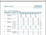
Well 14.95V according to this (presumably at 10mA as in the Texas Instruments datasheet):

HEF4081.jpg

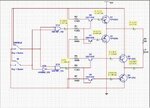
And, in my simulation, I have added some transistors between the logic output and darlington bases as buffers (is that what you would call them in this situation?) to keep the power dissipation of the logic chip within limits.

Do you have any other suggestions about the circuit?

GateDriver__.jpg

I used multim 12 for this simulation as it seems to have a wider range of components including the TIP120 and TIP125.
 
Last edited:

Can you specify the actual GDT lamp?

Gas Discharge Tube lamps don't have a low impedance at low voltage unless it includes an autotransformer to trigger the tube at 1kV. These nonlinear negative resistance characteristics are essential characterizing the VI vs t power responses with specular resonant effects.

HC logic has a driver impedance from 200 to 1000 depending Vcc and supplier.

overall, this is a poor topology for driving GDT lamps.
 

Well 14.95V according to this (presumably at 10mA as in the Texas Instruments datasheet)
The datasheet says the output current is less than 1uA!. The graph shows with a 15V supply and a 10mA current the output voltage is only ... wait a minute, you show the graph for the minimum currents, the typical currents are double.
With a 15V supply and a 10mA current the typical output voltage is +13V.

And, in my simulation, I have added some transistors between the logic output and darlington bases as buffers (is that what you would call them in this situation?) to keep the power dissipation of the logic chip within limits.
Do you have any other suggestions about the circuit?
The transistors add even more voltage loss.
The collector resistors are not needed because the transistors are emitter-followers.
The base currents for the darlingtons are so low that the transistors are also not needed.
 

Can you specify the actual GDT lamp?

Gas Discharge Tube lamps don't have a low impedance at low voltage unless it includes an autotransformer to trigger the tube at 1kV. These nonlinear negative resistance characteristics are essential characterizing the VI vs t power responses with specular resonant effects.

HC logic has a driver impedance from 200 to 1000 depending Vcc and supplier.

overall, this is a poor topology for driving GDT lamps.
Sunny I am trying to drive a gate drive transformer rather than a gas discharge tube.

- - - Updated - - -

The datasheet says the output current is less than 1uA!. The graph shows with a 15V supply and a 10mA current the output voltage is only ... wait a minute, you show the graph for the minimum currents, the typical currents are double.
With a 15V supply and a 10mA current the typical output voltage is +13V.


The transistors add even more voltage loss.
The collector resistors are not needed because the transistors are emitter-followers.
The base currents for the darlingtons are so low that the transistors are also not needed.

How would you interface logic chips with a transistor then audio? I have not been able to find any examples other than using them to drive a led.


How would you interface logic chips with a transistor then audio?
It is confusing since you have two threads about this circuit.
On your other thread I calculated a few things from spec's on the datasheets and showed an example that the output from the CD4081 can directly drive the 3mA inputs of the darlingtons with a half volt loss and no heating.
 

is less than 1uA

Audio I don't understand where you are getting that from.

I was looking at this graph that says there is typically a output high current of 30mA

Graph_.jpg

At the same time I can see in my simulation that the ANDs are outputting about 20uA at 15V, inline with what you are telling me, once I removed the collector resistors as you suggested.

- - - Updated - - -

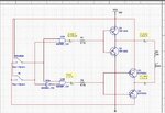
I tried removing the transistors and more or less the darlington base resistors and my simulation shows this improvement. The darlingtons only drop 2V now. According to the TIP datasheet 2V is saturated but it indicates a base current of 12mA for this. So my simulation TIPs must have a higher gain than what the datasheet says?

If I don't have some darlington base resistance value, the simulator wont display the current from the AND for some obscure reason.

GateDriver___.jpg

But I still don't get why the AND is not outputting 30mA at 15V as this graph in the texas instruments datasheet seems to suggest to me:
Graph_.jpg
 
Last edited:

Audio I don't understand where you are getting that (1uA) from.
The written spec says that with a 15V supply its output high voltage is 14.95V when its output current is less than 1uA.

I was looking at this graph that says there is typically a output high current of 30mA.
But I still don't get why the AND is not outputting 30mA at 15V as this graph in the texas instruments datasheet seems to suggest to me:
That is when its load is a short circuit to ground. Then the output resistance of the output transistor has the entire supply voltage across it so the current and heating are the highest.

At the same time I can see in my simulation that the ANDs are outputting about 20mA when the supply is 15V, inline with what you are telling me, once I removed the collector resistors as you suggested.
Then the Sim does not agree with the graph. Your new Sim also does not agree since the output current from the CD4081 shows only 2.75mA which does not agree with the datasheet value of a current gain for the darlingtons at 3A of 1000.

According to the TIP datasheet 2V is saturated but it indicates a base current of 12mA for this. So my simulation TIPs must have a higher gain than what the datasheet says?
Multisim is stupid. It doesn't know that an emitter-follower does not saturate!. A common-emitter transistor or darlington saturates with a lower current gain than when it is linear emitter-follower.

If I don't have some darlington base resistance value, the simulator wont display the current from the AND for some obscure reason.
Because Multisim is Stupid.
 

The written spec says that with a 15V supply its output high voltage is 14.95V when its output current is less than 1uA.


That is when its load is a short circuit to ground. Then the output resistance of the output transistor has the entire supply voltage across it so the current and heating are the highest.


Then the Sim does not agree with the graph. Your new Sim also does not agree since the output current from the CD4081 shows only 2.75mA which does not agree with the datasheet value of a current gain for the darlingtons at 3A of 1000.


Multisim is stupid. It doesn't know that an emitter-follower does not saturate!. A common-emitter transistor or darlington saturates with a lower current gain than when it is linear emitter-follower.


Because Multisim is Stupid.

Audio forgive me if I am being a total doofus but I am reading this from the texas instruments datasheet:

Table.jpg
Can you explain to me, in terms that an amateur is likely to understand, how or where you are getting 1uA from.

Because Multisim is Stupid.

OK well, even as an amateur I can recognize that there are issues with Multisim.

What simulator do you use?

At least according to the table above, the current flow indicated by Multisim seems ball parkish. But clearly I am going to need to check things with my multimeter before I permanently solder anything to my darlington bases.


Ooooh I think I get what you are saying Audio.

I am getting confused between this

Table.jpg

and this:
Table_.jpg

OK so the AND puts out perhaps 13V at 6mA, or so, if shorted to GND.

So what is it likely to put out if connected to a darlington base?

- - - Updated - - -

Trying to make better sense of what the datasheet is telling me.

OK so the AND puts out a minimum of 13.5V at 6mA.

Therefore it can put out a maximum of 37mA at 13.5V until it starts to burn up.

Is that right?

So we need a base resistor to limit the current to the 20mA needed by the darlington base.

If yes then why is it inadequate to drive the darlington?

How would you drive a darlington from a logic chip?
 
Last edited:

Can you explain to me, in terms that an amateur is likely to understand, how or where you are getting 1uA from.
It is clearly printed on the datasheet. The output of a Cmos logic IC is designed to drive the input of another Cmos logic IC. The input draws NO current.

OK well, even as an amateur I can recognize that there are issues with Multisim.
What simulator do you use?
I use LTspiceIV simulator but only on forums. I design a circuit using spec's for the devices from their datasheets observing minimums and maximums. Then every circuit works perfectly. Most of my projects were custom and no solderless breadboard was used.
I built and tested the prototype and it was what was sold and installed for the customer.

At least according to the table above, current flow indicated by Multisim seems ball parkish.
It looks like Multisim cannot read datasheets.

OK so the AND puts out perhaps 13V at 6mA, or so, if shorted to GND.
You make no sense. How can the output be at +13.5V when it is shorted to ground?
When the load to ground is 6.8mA then the output is about +13.5V. When the output is shorted to ground then the graph shows 30mA.

So what is it likely to put out if connected to a darlington base?
I worked it out already in this or in the other thread.

The darlington is an emitter-follower that NEVER saturates so its minimum current gain at an output of 3A is 1000 then its maximum input current is only 3mA not 20mA!
With an output current of only 3mA then the output voltage of the CD4081 that has a 15V supply is about 14.5V which is the input to the darlington. The base-emitter voltage drop of the darlington at 3A is about 2V so its output will be about +12.5V.
The PNP darlington will also have a voltage drop of (15V - 12.5V=) 2.5V then the 2 ohms load gets 12.5V - 2.5V= 10V. Then the actual output current will be a little less than (10V/2 ohms=) 5A instead of the calculated 3A.

OK so the AND puts out a minimum of 13.5V at 6mA.
Yes, but we do not need 6.8mA, we need only 3mA so the output voltage will be higher than 13.5V as shown on the graph.

Therefore it can put out a maximum of 37mA at 13.5V until it starts to burn up.
Impossible!
Its output current is shown as 30mA when its output high is shorted to ground and is 0V. Then it heats with 15V x 30mA= 450mW but its maximum allowed dissipation is only 100mW.
Your CD4081 with an output of 14.5V and a current of 3mA heats with only (15V - 14.5V) x 3mA= 1.5mW.

So we need a base resistor to limit the current to the 20mA needed by the darlington base.
The darlington as an emitter-follower never saturates so its maximum input current will be about 3mA not 20mA!.
A resistor is needed only if the output of the darlington is shorted to ground causing its input current to be very high. Then the darlington will burn up but not the CD4081.
 

Attachments

  • 14.95V with less than 1uA.png
    14.95V with less than 1uA.png
    150.6 KB · Views: 92
  • Cmos voltage and current limits.png
    Cmos voltage and current limits.png
    34.3 KB · Views: 99

OK Audio I have read this **broken link removed** and I think I have my head around what you are trying to tell me.

My totem pole is an emitter follower where the Vout is Vin - 1.4 in the case of a darlington transistor but with substantial current gain (needed to charge and discharge the FET gate capacitance quickly). Or in my case drive a GDT.

I want enough base current to saturate the darlingtons in this situation, but you are saying that the AND cannot supply it without overheating. And even if it could supply the required 12mA, it can't do it at 15V, and my GDT would have to have a primary to secondary turns ratio greater than what I currently have to make up for the loss in voltage.

So than how then how is it possible to replicate the functionality of a UCC27425, with its Vin and Venable, using logic gates?

Or is it, to all amateur intents and purposes, it is simply not possible?

- - - Updated - - -

Unless I use the UCC27425 to drive the my totem poles rather than my GDT, and then let the totem poles supply the large drive current for the GDT.

UCC27425 is perhaps designed to drive the smaller FETs with quite low current requirements.

From is max continuous current in the data sheet, it could certainly handle a continuous 30mA or so and at close to 15V.

Would you regard that as a better topology?
 

Status
Not open for further replies.

Part and Inventory Search

Welcome to EDABoard.com

Sponsor

Back
Top