Continue to Site

Welcome to EDAboard.com

Welcome to our site! EDAboard.com is an international Electronics Discussion Forum focused on EDA software, circuits, schematics, books, theory, papers, asic, pld, 8051, DSP, Network, RF, Analog Design, PCB, Service Manuals... and a whole lot more! To participate you need to register. Registration is free. Click here to register now.

Reference voltage generation for opamp

Status
Not open for further replies.

viperpaki007

Full Member level 5
Full Member level 5
Joined
Jul 2, 2008
Messages
274
Helped
11
Reputation
22
Reaction score
8
Trophy points
1,298
Location
Finland
Activity points
3,437
Hi,

I need to generate three bias voltages 600mV, 500mV and 450mV for the opamp shown in the attached diagram. Can somebody suggest a way to generate these reference voltages so that the generated voltages are independent of temperature and process variations.


regards
 

Attachments

  • opampv4.png
    opampv4.png
    48.5 KB · Views: 232

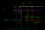
Try something like the schematic shown in the image. Here I am taking 5uA reference current, converting it into a 1uA current and then generating the references for the 1uA current. You can change according to your need.
The different colours mark the different bias lines.
As long as the input bias current is constant, the bias voltages would correspond to it ie it would track across process and temperature.
Also the sizes should match with what you have in your circuit for the best matching.

For the size of the cascode bias generators namely mpb21/mpb22 and mn10/mn13, the size of the bottom device(mpb21/mn10) should be about 1/3 of the size of the top device(mpb22/mn13). You can derive this since the bottom devices are in triode.

biasing2.png
 
Are you provided an external absolute reference of any kind?
If not then you're not going to be free of temp and make
tolerances without creating your own bandgap reference and,
depending on the accuracy goals, perhaps a trimmable one.
 

I understand that you are asking how to generate the reference itself? If so, how about reviewing IC design text books about band gap circuits?
 

Can you explain the benefits of cascode bias generators for DC bias generation? I know self cascode transistor has longer equivalent L and larger output impedance. How to relate this characteristic to DC bias generation? Also, can you provide more details on why the bottom device size should be about 1/3 of top device size?


Try something like the schematic shown in the image. Here I am taking 5uA reference current, converting it into a 1uA current and then generating the references for the 1uA current. You can change according to your need.
The different colours mark the different bias lines.
As long as the input bias current is constant, the bias voltages would correspond to it ie it would track across process and temperature.
Also the sizes should match with what you have in your circuit for the best matching.

For the size of the cascode bias generators namely mpb21/mpb22 and mn10/mn13, the size of the bottom device(mpb21/mn10) should be about 1/3 of the size of the top device(mpb22/mn13). You can derive this since the bottom devices are in triode.

View attachment 99423
 
Last edited:

Can you explain the benefits of cascode bias generators for DC bias generation? I know self cascode transistor has longer equivalent L and larger output impedance. How to relate this characteristic to DC bias generation? Also, can you provide more details on why the bottom device size should be about 1/3 of top device size?

The cascode current mirror forces the Vds of the current mirror devices to be the same and hence forcing the current to be same in both the arms. This is the biggest advantage but it comes a the cost of volltage headroom. Cascode is useful for mirroring currents on large ratios and is pretty accurate irrespective of the voltage at the drain of the cascode device. I have used cascode mirroring to convert 1uA to 200uA with a very good accuracy.

Look in the Gray/Meyer Book for such biasing schemes. The Jacob Baker Book also describes a few.
The idea is to provide the minimum bias voltages so as to maximize the output range of the amplifier. What I have shown is like a high swing cascode current mirror.
 
Hi niyishn5,

Can you explain the circuit a bit more. If the bottom transistors are acting as current mirrors then why they have to be in triode region and why there sizes should be 3 times smaller.

- - - Updated - - -

Hi FVM,

I already have a constant current reference source from outside of the IC. Now i need to generate constant bias reference voltages from this constant current source.
 

Hi niyishn5,

Can you explain the circuit a bit more. If the bottom transistors are acting as current mirrors then why they have to be in triode region and why there sizes should be 3 times smaller.

Hi,
Consider the NMOS Bias lines marked with the colours Red and Green.

The Red Line has to be Vov1 + Vth
and the Green Line has to be Vov1 + (Vth + Vov2)
for maximum swing.

For the transistors mn10 and mn13,
mn13 is in saturation and has gate voltage of Vov1 + (Vth + Vov2) (assuming the design was correct).
Hence the source of mn13 has to be at Vov1

Therefore the transistor mn10 has
Vgs = Vov1 + (Vth + Vov2)
Vds = Vov1

Hence it has to be in Triode region.
With Vov1 and Vov2, you can determine the W/L for mn11 and mn14/mn13
Solve the triode region equation for the above values of Vgs and Vds and you would get the relative value of W/L required for mn10 compared to mn13 and mn11.

You can use the same concept for the PMOS devices.
 
Status
Not open for further replies.

Part and Inventory Search

Welcome to EDABoard.com

Sponsor

Back
Top