anwarkb555
Newbie level 3

Hi,
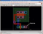
I am new to Cadance analog design flow. I am trying to buid a CMOS common source apmlifier. Library used is gdpk180nm. I have sussessfully built the circuit in Virtuoso Schematic editor and simulated it in ADE XL. When we try to do layout in Virtuoso Layout Suite, it is giving a DRC error "N+SD to Psub tap spacing must be <= 10.0 um". Assura DRC marks two locations with this error. Marked locations are the top region of source and drain of NMOS transistor. Not able to get any clue on this. Please help.
Thanks
Anwar

