Vinrys
Newbie

Hi, I am currently working on a project of 3 phase power inverter. The requirements are for it to be 20V input and 5 A output max. Now I have a few questions:
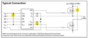
1) IR2110 components
I have a knowledge about bootstrap capacitor, why is it used etc. But in datasheet there are other capacitors (marked at the picture). Are they used to lower supply voltage fluctuations?
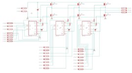
2) Voltage supply for drivers
Right now I have designed separate input pins for each driver, but since our supply voltage is 20V can I use it also to supply drivers (via connecting them on pcb). I will attach drawing of my circuit.
3) Transistors
Is IRF1404 right for the application? Its Vdss is 40 V and Vgs is 20 V so for me it seems so. What is disturbing is possibility for high Id (162 A). I know we want reach that amount but still, maybe there are other transistors better suited for this application.
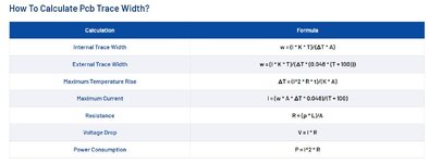
4) PCB trace width
I am searching for reliable formula for trace width. All I am seeing online are caltulators but I would like to know why and how. Best I have seen is this (attached file nr 3) but i wanted to see if its correct.
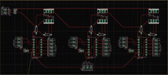
Also if you have any tips about pcb overall I would highly appreciate them. Thank you for your help.
1) IR2110 components
I have a knowledge about bootstrap capacitor, why is it used etc. But in datasheet there are other capacitors (marked at the picture). Are they used to lower supply voltage fluctuations?
2) Voltage supply for drivers
Right now I have designed separate input pins for each driver, but since our supply voltage is 20V can I use it also to supply drivers (via connecting them on pcb). I will attach drawing of my circuit.
3) Transistors
Is IRF1404 right for the application? Its Vdss is 40 V and Vgs is 20 V so for me it seems so. What is disturbing is possibility for high Id (162 A). I know we want reach that amount but still, maybe there are other transistors better suited for this application.
4) PCB trace width
I am searching for reliable formula for trace width. All I am seeing online are caltulators but I would like to know why and how. Best I have seen is this (attached file nr 3) but i wanted to see if its correct.
Also if you have any tips about pcb overall I would highly appreciate them. Thank you for your help.