Continue to Site

Welcome to EDAboard.com

Welcome to our site! EDAboard.com is an international Electronics Discussion Forum focused on EDA software, circuits, schematics, books, theory, papers, asic, pld, 8051, DSP, Network, RF, Analog Design, PCB, Service Manuals... and a whole lot more! To participate you need to register. Registration is free. Click here to register now.

2n7000 reverse D-S in DC or AF?

Status
Not open for further replies.

neazoi

Advanced Member level 6
Joined
Jan 5, 2008
Messages
4,134
Helped
13
Reputation
26
Reaction score
15
Trophy points
1,318
Location
Greece
Activity points
37,023
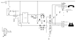
Hi I have a 2n7000 and I want to use it as a switch for small signal AF and low current DC. But In my application I do not know the direction of the DC and the AF signals.
So my question is, can the Drain and Source be reversed in this mosfet? i.e can DC and AC signals change polarity as they pass from the Drain to the Source and vice versa, or will the mosfet be destroyed?
 

As long as the gate to source voltage is high enough for the MOSFET to be on, signals will pass in both directions.
In the off state, the MOSFET will behave like a diode. If you want the MOSFET switch to be completely off in both directions, you can use 2 MOSFETs with the gates and sources connected together. The in/out will be the drains.
 

Yes, a MOSFET can conduct equally well in both directions when on.
But to block in both directions when off, you need to use two of them in series with back-to-back sources to prevent the parasitic source-drain diode from conducting.
To turn them off, you float the gates with a resistor (say 10k) between the source common connection and the gate common connection.

What are the signal voltages, and what supply voltages do you have available?
 

Better use JFET as bidirectional small signal switch, it has no substrate diode shorting reverse DS voltage.
 
Better use JFET as bidirectional small signal switch, it has no substrate diode shorting reverse DS voltage.

Components count is important so I think I will go that way and avoid having to use two devices for each switch. I have seen "mute" switches at the past using Jfets, but I do not like the negative voltage on the gate to switch them on, since there are only 0-5v available on the circuit.
Maybe I shall go for a P-type JFET which requires a positive gate voltage to switch them on?

- - - Updated - - -

Is the J177 a good choice for:

0v in the gate = switched on
5v in the gate = switched off

???
 

.....
Maybe I shall go for a P-type JFET which requires a positive gate voltage to switch them on?

- - - Updated - - -

Is the J177 a good choice for:

0v in the gate = switched on
5v in the gate = switched off

???
Note that the JFET gate voltage must be 5V higher than the maximum positive signal voltage to remain off.
What is that maximum voltage?

A CMOS switch might be a better choice, since it will switch a 0-5V signal with a 0-5V control and 5V supply.
 
Last edited:
  • Like
Reactions: neazoi

    neazoi

    Points: 2
    Helpful Answer Positive Rating
Note that the JFET gate voltage must be 5V higher than the maximum positive signal voltage to remain off.
What is that maximum voltage?

A CMOS switch might be a better choice, since it will switch a 0-5V signal with a 0-5V control and 5V supply.

I would like to go discrete. I would use relays but they consume some power and this will come close to the limits of my 78L05.
This will be used to switch off/on the AF signals and the DC (I measure 3.7v or so max) of a standard desktop telephone earpiece. You know, the part that you pick up and place to your ear when you want to make a call. This has a cable with 4 wires in it. Some wires carry both DC and AF, like the capacitive capsule mike.

So will the J177 do ok?

Here is the modem I have designed so far, which shows the J177 in place. Please comment.
 

Attachments

  • modem2.GIF
    modem2.GIF
    32.6 KB · Views: 151

The maximum Vgs cutoff voltage for the J177is 2.5V, which means the maximum signal you can block is 5V - 2.5V = 2.5V with a 5V control signal, thus it won't fully block your 3.7V signal.

So you either need a higher control voltage, or a JFET with a maximum Vgs cutoff voltage of less the 1.3V.

If neither of those are an option, then you need to consider a CMOS analog switch.
A SN74HC4066, for example, has four switches in one package, with an on-resistance of <100 ohms.
They are only about US$0.50.
 
Last edited:

Use a CD4016 or CD4066. Use one section as a switch or if you need better isolation, wire two sections in series and link their control signals. From the center connection wire the third switch to ground and use the fourth section as a control signal inverter. It will work off 5V, give better than 60dB off isolation and it will carry up to about 50MHz before losses become significant. One IC and one pull-up resistor is all you need. Current consumption will only be a few uA.

Brian.
 

The CD4016/4066 have a rather high on-resistance with a 5V supply, which is why I suggested the 74HC4066.
 

This biasing arrangement worked for my FET (2N3819), as I tried to turn it off by applying a negative voltage. Since it's a depletion mode fet, it needs to be biased in a different manner than our everyday transistors. I found that I had to obtain -1.7v relative to 0v ground. A simple way to do this was to put 2 AA batteries in series, and then dial to the correct value via 1 Mohm potentiometer.

**broken link removed**

If you don't wish to do the job with batteries, it is possible to derive a negative polarity supply from a positive, by using a charge pump circuit.

- - - Updated - - -

Similarly to turn off the P type fet requires 1.7v above the supply voltage. It would likewise require a pair of batteries, or a charge pump, or a boost converter.
 

Status
Not open for further replies.

Similar threads

Part and Inventory Search

Welcome to EDABoard.com

Sponsor

Back
Top