Continue to Site

Welcome to EDAboard.com

Welcome to our site! EDAboard.com is an international Electronics Discussion Forum focused on EDA software, circuits, schematics, books, theory, papers, asic, pld, 8051, DSP, Network, RF, Analog Design, PCB, Service Manuals... and a whole lot more! To participate you need to register. Registration is free. Click here to register now.

27MHz crystal oscillator transmitter simulation in PSPICE

Status
Not open for further replies.

viperpaki007

Full Member level 5
Full Member level 5
Joined
Jul 2, 2008
Messages
274
Helped
11
Reputation
22
Reaction score
8
Trophy points
1,298
Location
Finland
Activity points
3,437
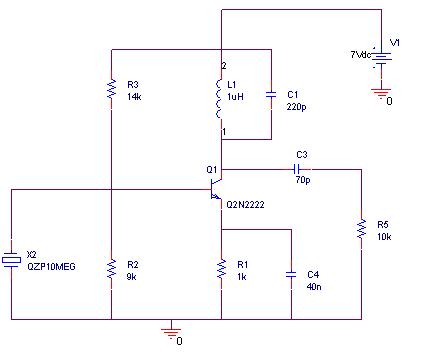
I want to simulate 27MHz transmitter circuit in PSPICE. Circuit diagram is given as Figure-1 in following link.
http://talkingelectronics.com/projects/27MHz Transmitters/27MHzLinks-1.html#Receiver for Tx_A

At the moment I am not including any antenna and just want to check the oscillations at transistor collector in PSPICE. Firstly, I am not able to find 27MHz xtal model in PSPICE. There is a xtal library in PSPICE with some xtals but I have no idea about their resonance frequency and how to edit the resonance frequency in the model. Where I can find the 27MHz xtal model for Pspice and also from where I can find the description for existing crystal models in PSPICE.

Moreover, how I will put the initial condition in PSPICE for the oscillations to start.

regards
 

Hello,

For the crystal go to https://en.wikipedia.org/wiki/Crystal_oscillator
Look to the image that shows an RLC series circuit with a parallel capacitor.

This circuit model is valid close to the resonant frequency of the crystal. Your 27 MHz may be a third overtone crystal, so it will also resonanate at one third of the frequency. To avoid this, your oscillator has some LC circuit to prevent oscillation at this low frequency. It can also be fundamental frequency, but I don't know

The Q factor for a crystal is very high. Assuming 30 Ohms series resonance impedance, you should think of Ls = 1.76 mH, Cs= 0.0196 pF, Rs = 28 Ohms for the RLC series circuit and Cp (that is the holder capacitance) about 12 pF.

When you put this model into your PSPICE circuit, it will take long time before you will see any oscillation. The reason for that is that the Q factor of the crystal is so high, that it takes thousands of RF cycles before the crystal shows sufficient mechanical oscillations. So depending on the loop gain in your oscillator, it may take 20 thousand RF periods before seeing significant output. If your oscillator oscillates within several hundreds of periods, you can be sure your oscillator does not oscillate at the crystal frequency.

To speed up oscillator start up, you may use initial conditions and start the simulator using initial conditions (so not from DC bias calculation). For Cs in the crystal model, you may start with 5kV (yes, 5 kilo Volt).

Normally I reduce the Q factor of the crystal by increasing Cs and reducing Ls, in combination with initial conditions.

Regarding how to set initial conditions, what pspice package do you use?

Hope this helps you a bit.
 
Thanks WimRFP for the information. It is quite helpful but some of my questions still remain unanswered.

1) If we have to use an electrical model of crystal resonator then why PSPICE has a separate library 'xtal' having some xtal components like QZP100K. What is their use?

2) From where I can find description of PSPICE library models. Some of the models are totally unclear to me that what is their use.
 

Are you able to look into the model (so that you can see the model parameters)?

If so it should mention things as "fundamental motional inductance, Lm", "fundamental motional capacitance, Cm", "fundamental motional resistance, Rm1" , for overtone use it may mention Rm2, Rm3 and of course the "holder capacitance, shunt capacitance".

QZP100K very likely is a 100 kHz crystal. If you know how to manipulate your database (that is copying pspice models, add new circuit representations, etc), you may make a new model based on an existing one. My pspice (Beige Bag) copies the model into the schematics and there I can play with the model parameters without overwriting my database.

Cm, Lm and Rm are the series components mentioned in the wiki link. C0 is the parallel capacitance.
 
Hi WimRFP,

No, I cannot look into the model. When I open the model parameters for editing, there are no options to edit Lm, Cm and other xtal parameters.

Moreover, when I try to use these components in simulations, they do not work at all. See my attached circuit diagram. There is no option to put any initial condition in xtal model.

77_1333964877.jpg


---------- Post added at 10:52 ---------- Previous post was at 10:48 ----------

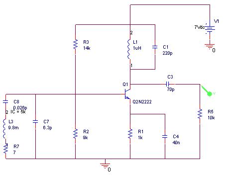
However, the above circuit works when i replace X2 with an electrical equivalent model of crystal and put an initial condition of 5kV on Cs of electrical model. The only error in the simulation results in higher output voltages upto 200V peak to peak which should not happen. Are this really the right output result..


---------- Post added at 10:54 ---------- Previous post was at 10:52 ----------

88_1333965248.jpg
 

If you can't change it, use your own model (as you did).

You may reduce the initial voltage, start with about 50V and let the oscillator run for very long time (several thousand RF periods), otherwise you can't judge your oscillator. The oscillator has 7 V supply, so output voltage should be less then 200V... Check that the oscillator is running at the crystal frequency (so it is not free running dictated by the collector resonant circuit).

You may know that this type of oscillator requires both the crystal and the collector resonant circuit to be inductive, as the feedback is via the collector base capacitance. So the resonant frequency of the collector tank circuit should be somewhat above the working frequency.

Do you have the specs for the crystal you are going to use (you use 7 ohms for Rs, that seems low)?

I am not able to understand your above sentence properly. Can you elaborate please. and I used the electrical model parameters from some internet link which i dont remember now. Do you know what will be the value for 27MHz crystal resonator and how to calculate them.
 

You can use the values I gave you before. The series circuit resonates at 27.125 MHz, so if your oscillator does work, it should provide a frequency just above 27.125 MHz.

If you are not familiar with how oscillators work, try to locate a document on oscillator basics. The oscillator you have is the transistor version of the oscillator that is called "tuned plate tuned grid (tptg)" oscillator or tuned drain tuned gate oscillator in case of a FET. This type of oscillator uses the capacitance between input and output as feedback (in your case the collector base capacitance).

Both base and collector needs to see an inductive load in order to get positive feedback. A crystal just above the series resonant frequency becomes inductive. Therefore your oscillator should oscillate just above the series resonant frequency of the LCR series circuit in your crystal model.
 

Hi WimRFP,

I am not able to find much information about this 'tuned drain tuned gate' oscillator from internet. Somewhere I read that this kind of oscillator is Colpitt oscillator but I am unable to match this circuit with basic colpitt oscillator configuration. Can you suggest any article which can tell this oscillator theory in general.
 

Hello Viperpaki007,

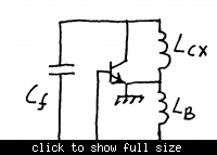
When the circuit oscillates, it can be simplified as shown below (all DC components not shown):


Here you can see that the LC network may provide180 degr. phase shift between collector and base (see it as a tapped LC resonator).
The transistor provides the other 180 degr. to get positive feedback. Note that the emitter is the common (ground)

Lb = formed by the crystal and the transistor's BE capacitance.
LCX is formed by your slightly inductive LC circuit (in the collector) together with the transistor's (low) CE capacitance.
Cf is the transistor's CB capacitance .

Regarding BE capacitance, this is not the one shown in the transistors's datasheet, but mainly the diffusion capacitance (that is larger then in the datasheet and depends on the collector current and ft).
 
How you have connected the emitter to ground.....There is a resistor of 390 Ohm and capacitor of 82pF attached to it. 82 pF cannot be considered as short at 27MHZ.

---------- Post added at 15:40 ---------- Previous post was at 15:19 ----------

I simulated the circuit with bigger value of emitter capacitor (so that its effect at 27MHz can be neglected) but the circuit stops oscillating.
 

Hello,

your posted circuits shows 40n.

I allready had my thoughts about such large value. That you use a much lower value is good.

Transistors have also parasitic inductance and parasitic resistance, especially the emitter lead induction has influence. This causes the phase shift introduced by the transistor to change in the wrong direction (adds some additional negative phase shift). Having some capacitive impedance in the emitter corrects this and gives better oscillation.

Increasing the emitter impedance gives a kind of mixed mode oscillator where feedback is provided both via Ccb and Ce. There is a change that you can get it running even without collector load (it then becomes a common collector cicuit where the collector is grounded for AC). If doing this, there is a risk of oscillation at fundamental frequency (if you use a third overtone crystal).
 
Status
Not open for further replies.

Part and Inventory Search

Welcome to EDABoard.com

Sponsor

Back
Top