Continue to Site

Welcome to EDAboard.com

Welcome to our site! EDAboard.com is an international Electronics Discussion Forum focused on EDA software, circuits, schematics, books, theory, papers, asic, pld, 8051, DSP, Network, RF, Analog Design, PCB, Service Manuals... and a whole lot more! To participate you need to register. Registration is free. Click here to register now.

[SOLVED] Reducing op amp ring when charging capacitor

Status
Not open for further replies.

jasonc2

Full Member level 4
Full Member level 4
Joined
Jun 23, 2012
Messages
204
Helped
25
Reputation
52
Reaction score
25
Trophy points
1,328
Location
NYC, USA
Activity points
3,415

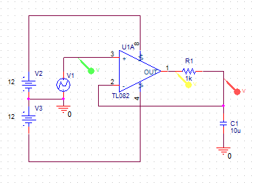
This circuit shows the input switching on and off and the voltage on the capacitor ramping up and down, exactly what is expected. As the capacitor and resistor would form a low pass filter with a relatively low cut off frequenct, I would not expect to see any ringing.
Frank
 

You can see the ringing in the color changes or by inspecting op amp output but here it is in PSpice:

Circuit:
5_1344280658.png


Overview:


Op amp output in yellow:


Detail @ 5V:


As the capacitor and resistor would form a low pass filter with a relatively low cut off frequenct, I would not expect to see any ringing.

The ringing makes sense to me because the op amp output initially overshoots, then when the capacitor approaches the target voltage it overcharges before output drops, and the op amp output falls low, and that cycle repeats. The low filter cutoff is the reason for the ringing because of the longer delay times. Lower cutoff (e.g. larger capacitor) actually leads to higher magnitude ringing.
 

Try putting a 10 ohm resistor inline with the capacitor. That restores proper response (shown as a single stable color transition at the output of the op amp).

Notice if you use a 1 ohm resistance, the ringing returns (seen as rapid flashing red and green at the output).

The ringing we see is because the simulator exaggerates a tiny discrepancy in response among the various components, from one iteration to the next. (Falstad's simulator is not alone in having limitations.) This is likely where we put a plain capacitor adjacent to plain wires, often bringing out such jittery response in a simulator.

Come to think of it, the ringing we see could in fact be occuring in real life, but at a speed of femtoseconds, much more quickly than the eye can see. Hence the time needed for node levels to settle is usually transient and of little consequence.

A simulator, however, due to calculating from one discrete step to the next, might generate these real behaviors artificially, yet distort their timeframe, and their influence.
 
  • Like
Reactions: jasonc2 and FvM

    FvM

    Points: 2
    Helpful Answer Positive Rating

    jasonc2

    Points: 2
    Helpful Answer Positive Rating
I have some doubts if the Falstad simulator represents the OP behaviour accurately in this situation, the PSpice models usually do.

The basic problem is simple, zero respectively negative phase margin in the loop gain characteristic. If the OP compensation isn't accessible for modifications, you have basically two option:

- an output series resistor to isolate the capacitor, as suggested by BradtheRad. The main disadavantage is (at least in some situations) is the DC error introduced by the resistor, e.g. for an accurate reference voltage buffer with some load current

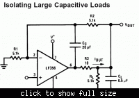
- a series resistor with additional DC feedback path, as in the below application circuit. The DC error is cancelled, but the phase margin (and respective transient behaviour) isn't very good


By personal favourite in most situation is a fast OP (> 100 MHz GBW) and a very small series resistor (e.g. 0.1 ohm), or in some cases a fast OP with resistor and additional DC feedback.

P.S.:
Come to think of it, the ringing we see could in fact be occuring in real life, but at a speed of femtoseconds, much more quickly than the eye can see.
I don't agree about the femtoseconds. The ringing occurs near the loop gain unity gain frequency. Without isolating resistor, the OP output stage will still cause an oscillation frequency in the middle to upper khz range for larger capacitors. So it will be observable with an oscilloscope, although the oscillation magnitude can be low in some cases.
 
Last edited:
Attached is a circuit similar to that of FvM's but with an added capacitor across R2. I empirically and somewhat arbitrarily selected the component values to give a Bode plot with no significant peaking and good phase margin. They are not necessarily optimum values. The transient response is good with no sign of ringing at the op amp output.

Op Amp Cap Drive.gif
 
  • Like
Reactions: jasonc2

    jasonc2

    Points: 2
    Helpful Answer Positive Rating
Interesting, thanks guys.

I had presumed it had something to do with the op amp slew rate but in thinking about Bradtherad's comments in post #4 I did the math (hopefully correctly) find the capacitors charge rate when it crosses the target threshold, assuming the op amp stays saturated. For charging, in my original circuit, with the op amp at ~11.3V and the target at 5V, based on the formula i(t) = C * dV / dt, I got:

dV / dT = i / C = (11.3V - 5V) / (1000Ω) / (10µF) = 0.00063 V/µs

Which is well below the TL082's 13 V/µs slew rate, which means the op amp is more than capable of keeping up with the capacitor, so my presumption was incorrect, or at least it didn't account for the magnitude of what I saw. This supports all of the comments above.

Adding a 100Ω series resistor cleaned it up. Is that a real life issue or just a simulator fix? Adding only capacitor ESR e.g. a 20mΩ series resistor slightly reduced but did not eliminate the ringing.

I will study the circuits FvM and and crutschow posted more.

I have another question:

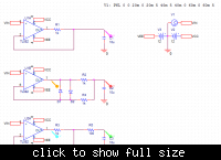
Before I saw any replies here I tried a different circuit. I figured it might help to not let the op amp output go quite as far past the target voltage, so I added some diodes, the center circuit below:


This also cleaned up the output but not as cleanly as simply adding a resistor (op amp output = orange, capacitor voltage = red -- the resistor circuit is blue/green by comparison):


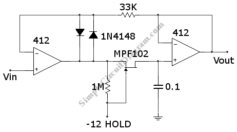
When I did this, I thought the circuit looked familiar, then I remembered seeing the same set up in a sample-and-hold circuit I was looking at a few days ago:

LM412-Sample-and-Hold.gif


My question is: If the issue with the ringing is primarily a discrete simulator issue, is it possible the designer of that circuit observed the ringing in a simulator and coincidentally came up with the same "solution" that I did? Or does the clamping in that circuit actually address a real life issue? A Google image search for sample and hold yields a few other circuits with the diode configuration, but the vast majority do not have them.

Thanks!
 

No it's not a simulator issue. The oscillations are due to the phase shift caused by the RC output which generates positive feedback at the ringing frequency. A series resistor reduces the feedback phase shift and eliminates the instability.

The diodes limit the capacitor slew rate which apparently minimizes the instability problem (and also slows down the charge rate of the capacitor).
 
  • Like
Reactions: jasonc2

    jasonc2

    Points: 2
    Helpful Answer Positive Rating
This is not ringing, its RF instability or squegging. There are no "rings" on the leading edge of the output waveform. What is the "5V detail" all about?, this looks like RF to me and is not related to the input waveform? or have you changed the timebase speed?
Frank
 

This is not ringing, its RF instability or squegging. There are no "rings" on the leading edge of the output waveform. What is the "5V detail" all about?, this looks like RF to me and is not related to the input waveform? or have you changed the timebase speed?
Frank
I thought it was RF too until I enlarged the image. The time base scale looks like ns but is actually ms.
 

I had presumed it had something to do with the op amp slew rate but in thinking about Bradtherad's comments in post #4 I did the math (hopefully correctly) find the capacitors charge rate when it crosses the target threshold, assuming the op amp stays saturated. For charging, in my original circuit, with the op amp at ~11.3V and the target at 5V, based on the formula i(t) = C * dV / dt, I got:

dV / dT = i / C = (11.3V - 5V) / (1000Ω) / (10µF) = 0.00063 V/µs

Which is well below the TL082's 13 V/µs slew rate, which means the op amp is more than capable of keeping up with the capacitor, so my presumption was incorrect, or at least it didn't account for the magnitude of what I saw. This supports all of the comments above.

Non-linear effects, e.g. slew-rate and output current limiting will surely modifiy the circuit behaviour. There are even some cases, where instability isn't brought up without non-linear effects. But before you study these "advanced" problems in your circuit, you should really refer to the basic ones, "simple" problems of feedback loop stability that can be already seen in a small signal analysis.

Adding a 100Ω series resistor cleaned it up. Is that a real life issue or just a simulator fix? Adding only capacitor ESR e.g. a 20mΩ series resistor slightly reduced but did not eliminate the ringing.
It's a distinct real life issue. And as already explained, not cleaned up by 20 or even 500 mohm ESR. But this are details you should try yourself.
 
  • Like
Reactions: LvW and jasonc2

    jasonc2

    Points: 2
    Helpful Answer Positive Rating

    LvW

    Points: 2
    Helpful Answer Positive Rating
This is not ringing, its RF instability or squegging. There are no "rings" on the leading edge of the output waveform. What is the "5V detail" all about?, this looks like RF to me and is not related to the input waveform? or have you changed the timebase speed?

It's zoomed in on the plot, to show detail, up around 5V. I called it ringing because it decreased in amplitude over time but maybe that was the wrong term.

- - - Updated - - -

But before you study these "advanced" problems in your circuit, you should really refer to the basic ones, "simple" problems of feedback loop stability that can be already seen in a small signal analysis.

I don't have much knowledge of feedback control systems, do you have a favorite introductory resource you can recommend? Preferably something medium- to fast-paced.

- - - Updated - - -

Also, for more complex control loops, are there any good general "rule-of-thumb" techniques for isolating the cause of such instability? I am finding it difficult because the effect appears throughout the entire loop so it's hard to identify initial causes, and my usual approach of removing problematic parts and isolating the failure falls apart with feedback loops.

Thanks!
 

I called it ringing because it decreased in amplitude over time but maybe that was the wrong term.

Jason - I think, it is the correct term. Perhaps that's only a word - and not to important. On the other hand - using false terms creates misunderstandings.
What is ringing?
Answer: When the step response exhibits a decaying oscillatory behaviour over several periods (less than one period would be called "overshoot").
And this behaviour is caused by a stability margin which may be considered as not sufficient.

- - - Updated - - -

Also, for more complex control loops, are there any good general "rule-of-thumb" techniques for isolating the cause of such instability? I am finding it difficult because the effect appears throughout the entire loop so it's hard to identify initial causes, and my usual approach of removing problematic parts and isolating the failure falls apart with feedback loops.
Thanks!

Cause of instability? In case of so called "dynamic instability" the reason is a small stability margin which is defined for the frequency-dependent loop gain function.
In this case, the classical criteria from BODE and NYQUIST are to be mentioned.
Since all loop components contribute to the total loop phase, you cannot identify one particular part or unit that is solely "responsible" for such a behaviour.
In such a case, two methods can improve the situation in principle:
1.) Placement of an additional block (compensator) or part that is able to enhance the phase in the critical frequency region,
2.) Modification of any part or block within the loop with the same target.
 
  • Like
Reactions: FvM and jasonc2

    jasonc2

    Points: 2
    Helpful Answer Positive Rating

    FvM

    Points: 2
    Helpful Answer Positive Rating
Since all loop components contribute to the total loop phase, you cannot identify one particular part or unit that is solely "responsible" for such a behaviour.

Good point, this is fundamentally why my approaches so far have been failing.

Good advice all around, thank you.
 

To view the stability behavior of the loop you can do an AC analysis to generate a gain and phase plot with frequency. My simulations of that showed a pronounced peak in the gain near the observed ringing frequency. From that I tried some different feedback compensation approaches until I eliminated the peak, giving a flat response up to the rolloff point (shown in the Bode plot) with good phase shift margin. This is the circuit shown in my post #6.

It's difficult to determine what's happening in a feedback loop without doing gain-phase (Bode) plots. Here's a primer on that.
 
  • Like
Reactions: jasonc2 and FvM

    FvM

    Points: 2
    Helpful Answer Positive Rating

    jasonc2

    Points: 2
    Helpful Answer Positive Rating
To view the stability behavior of the loop you can do an AC analysis to generate a gain and phase plot with frequency. My simulations of that showed a pronounced peak in the gain near the observed ringing frequency.

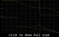
Oh neat. Here is phase (top) and frequency (bottom) response for the three circuits I posted above (green is original, red is with diodes, yellow is with resistor):


That's pretty cool. So I guess, it's like a filter and it amplifies that frequency in the step input, and so I see oscillations at that frequency at the output?

I put a notch filter in at that frequency to see what would happen, but it just moved the oscillation to a different frequency.

I am now reading this document, it seems like a good intro: **broken link removed**

Why is it that the gain peak appears at the same frequency as the phase transition?
 

When the loop phase shift approaches 180 degrees, the feedback becomes positive, which causes peaking and oscillations, thus the phase transition and the peaking frequency are coincident.

Yes, the step input has high frequency harmonics, which excite the ringing frequency.

The notch filter introduces its own phase shifts which just causes the phase inversion and peaking to occur at a different frequency. The Bode plot will show that.

To eliminate the peaking you need a network that cancels the sharp phase shift change. The two capacitors and resistor added to the circuit in post #6 perform that function. If you simulate that circuit and vary the values of the capacitors, you will see how the peak changes value and moves in frequency.

Your referenced document looks like a good intro to feedback control systems.
 
  • Like
Reactions: jasonc2

    jasonc2

    Points: 2
    Helpful Answer Positive Rating
Although the ringing behaviour can be guessed from the closed loop gain bode plot, the cause can be seen better in the open loop bode plot. Even more important, the open loop caracteristic allows to design effective contra-measures, as previously discussed.
 
  • Like
Reactions: jasonc2

    jasonc2

    Points: 2
    Helpful Answer Positive Rating
Hi crutschow, sorry - but I am not "very happy" with your explanations. May I give my comments?

When the loop phase shift approaches 180 degrees, the feedback becomes positive, which causes peaking and oscillations, thus the phase transition and the peaking frequency are coincident.

I suppose, jason speaks about the closed-loop phase transition - in contrast to crutschow who apparently refers to the open-loop response.
Thus, jason's question has nothing to do with loop phase shift 180 deg. The sharp phase transition and the gain peaking are closely related because there is ALWAYS a fixed relation between gain and phase (for minimum phase systems without RHP zeros) - also for less peaking and a more smooth phase response. This has been shown by BODE long time ago.

Yes, the step input has high frequency harmonics, which excite the ringing frequency.

When a circuit suffers from a small phase margin there is no step input necessary to cause oscillations (decaying or not). That means: Not the "higher harmonics" excite the oscillations.
Each initial condition that is outside the equilibrium state will cause these oscillations - until the equilibrium state is reached.
By the way: It is also a common misconception that in oscillator circuits the noise will initiate oscillations.

To eliminate the peaking you need a network that cancels the sharp phase shift change.
This "sharp phase shift" is not the cause of the peaking effect. Instead, both effects are closely related and are caused by the loop gain which has a small phase margin.
Thus, improve the margin and the peaking will be eliminated.
 
  • Like
Reactions: jasonc2

    jasonc2

    Points: 2
    Helpful Answer Positive Rating
Status
Not open for further replies.

Similar threads

Part and Inventory Search

Welcome to EDABoard.com

Sponsor

Back
Top