Continue to Site

Welcome to EDAboard.com

Welcome to our site! EDAboard.com is an international Electronics Discussion Forum focused on EDA software, circuits, schematics, books, theory, papers, asic, pld, 8051, DSP, Network, RF, Analog Design, PCB, Service Manuals... and a whole lot more! To participate you need to register. Registration is free. Click here to register now.

need help to design FET based amplifier

Status
Not open for further replies.

harikrishnam

Junior Member level 3
Joined
Jul 8, 2011
Messages
28
Helped
0
Reputation
0
Reaction score
0
Trophy points
1,281
Activity points
1,465
hi to everybody,i very much interest to know how to design FET based amplifier.i know BJT design and op-amp design but FET design i don't know.i searched in the net according to their methods some parameters are required but those parameters are not available in datasheet if any body knows please help me.my major application is audio amp like equalizer or preamp or power amp.
 

Dear harikrishnam
Hi
What kind of fet amplifier ? CD ? CS ?CG ?
Best Wishes
Goldsmith
 

Dear harikrishnam
Hi
What kind of fet amplifier ? CD ? CS ?CG ?
Best Wishes
Goldsmith

Thank u so much for u r interest on my thread.if possible i want to know all above designs if it is not possible at least guide me about CS amplifier.if possible take bfr30 as FET and explain.Thanks in advance.

- - - Updated - - -

- - - Updated - - -

Are you interested in low power signal amplification or high power output stages (or both)?

possible both design i interest.
 

Hi again
Before start , tell me , please that are you familiar with AC equivalent circuit of each one ?
Best Events
Goldsmith
 

....some parameters are required but those parameters are not available in datasheet....
This is a problem with JFETs and MOSFETs, and it makes design more difficult than with BJTs.

Let's look at power MOSFETs first.

For a power amplifier, if you want to use a class AB push-pull source follower output stage, there is a small problem with the biasing because the gate-source threshold voltage of the MOSFETs can vary over such a wide range.

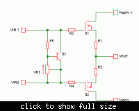
However, you can still use a Vbe multiplier, as you would with a bipolar output stage. The only difference is you need to allow a much wider adjustment range than normal, to allow for the unknown Vgs. It is also important to include gate stopper resistors to prevent oscillation. The picture below shows an output stage using a BJT for the Vbe multiplier. You could replace Q3 with another MOSFET. That should give better temperature compensation.

If you want to use parallel output devices for a high power amp, you have a big problem. With parallel BJTs, you can just use small emitter resistors to equalize the currents, but with MOSFETs this is not enough - the devices need to be matched. This means buying more MOSFETs than you need, measuring them, and using matched pairs.

This is also why it's often difficult and expensive to repair high power car amplifiers. Even if only a couple of MOSFETs are blown, a whole set of MOSFETs has to be replaced with matched devices. If you don't do that, the repair won't last long.

More later....

 
Last edited:

Now lets look at how to use JFETs for small signal circuitry.

The three main differences between JFETs and BJTs are:
  1. Almost no current flows into a JFET gate, so we don't have to worry about current gain.
  2. BJTs require a forward voltage of about 0.7V between base and emitter to switch them on. JFETs conduct a high current with zero voltage between gate and source. They are normally run at a lower current, with a reverse bias voltage between gate and source.
  3. The transconductance of JFETs is generally much lower than BJTs, running at the same current.
The first two can make biasing very easy and allow us to build very simple circuits. For example, this picture shows a simple common source voltage amplifier and a unity gain buffer.


Choosing the parts can be difficult, though. For example, if we want no DC at the output of the buffer, we must either make sure that the two JFETs have exactly the same Vgs, or we must use different values for the source resistors.

However there is a problem: We cannot tell from the datasheet what the Vgs of the JFETs will be, it can vary over a wide range. So for the first option, if we want two JFETs with the same gate-source voltage, we will have to buy more JFETs than we need, measure each one, and choose two that match.

For the second option, we only need to buy two JFETs but we will still need to measure them before we can decide what value resistors to use.

Looking at the buffer circuit again, we can see that there is a much easier way. If we just add a coupling capacitor at the output, there is no problem with DC, and we don't need to measure any JFETs.

This is an important lesson. When we are working with JFETs, we will often find ourselves having to measure, match and select individual JFETs unless we can design our circuits in such a way that big differences in JFET parameters do not have much effect.

This is not always as easy as it sounds. What if we want to use a differential pair (also called a long tailed pair or LTP) for the input stage of a power amplifier? How do we make sure there is no DC voltage across the loudspeaker?

We could put a big coupling capacitor at the output of the amplifier, but there may be good reasons why we don't want to do that. In that case, it looks like we really so need carefully matched JFETs for the input stage, unless we can think of some other trick to get rid of the DC.

In this case, the easy way is to use a trimmer potentiometer to adjust the DC voltage at the output to zero. This is a good solution but we must be careful how we use the trimmer in the circuit. Remember that trimmers (and other potentiometers) are not very reliable. If the wiper becomes disconnected we do not want to have the whole power supply voltage across the loudspeaker as this will destroy it. We must design the circuit in such a way that there will be no more than a couple of volts across the speaker if the trimmer fails.

If you look back at the MOSFET output stage I showed earlier, you will see a similar precaution. In that circuit, if the trimmer fails open circuit, bias is removed from the MOSFETs. There will be some distortion of the audio but nothing will be damaged.

If we swap the position of R5 and the trimmer, we can still adjust the bias to the correct value, but it will be a very bad design. If the trimmer fails, the MOSFETs will be overbiased, very high current will flow through them, and they will probably be destroyed.
 

Sorry, I think I made a mistake.

...i know BJT design and op-amp design but FET design i don't know...
When I saw that, I understood that you already know how to design circuits with BJTs and opamps. I thought that you only need to learn the difference between FET design and BJT design.

But now I see that you asked the previous day how to design a circuit with BJTs and opamps, so perhaps you do not know how to do that either?
 

Dear godfreyl
Hi
I think your circuit has a little problem . you should use a resistance in parallel with GS junction . isn't it ?
Best Regards
Goldsmith
 

I think your circuit has a little problem . you should use a resistance in parallel with GS junction . isn't it ?
I don't think so, but which circuit are you referring to? Why do you think there should be another resister?
 

As you know , each Mosfet is isolated ( i'm talking about Gate ) , and each mosfet has a capacitor in GS junction . when this capacitor be full of charge there won't be any path to discharge . it is exactly thing that the simulator is unable to show you . you can test it in practice too . use a battery and tester to test it !
Hence the THD will increase and the efficiency will decrease .
Best Luck
Goldsmith
 

As you know , each Mosfet is isolated ( i'm talking about Gate ) , and each mosfet has a capacitor in GS junction . when this capacitor be full of charge there won't be any path to discharge .
Yes this is true for the transistors having large gate capacitance and hence need some big resistance from gate to source. But normal design where gate capacitance is not large and even a digital signal can discharge this. Then no need to use resistance path. ( by large gate capacitance means more than 10pF)
 

goldsmith,
Are you talking about this circuit?


The gates in that circuit are voltage driven. There is no problem sucking the charge out of the gates. Adding a resistor between the gate and source of each MOSFET would serve no purpose.
 

Dear varunkant2k
Hi
Of course it's value is pretty low , but it is enough to keep on your mosfet ,
Best Regards
Goldsmith
 

I guess goldsmith is referring to one of the complementary source follower subcircuits in post #6 (enhancement MOSFET with bias source) or post #7 (JFET).

They don't need GS resistors, the output can be expected to follow the input with a gain < 1, depending on the RL to gm relation. Of course Cgs shows in the amplifier frequency characteristic.

It's not actually clear to me if the circuits are answering the rather unspecific questions of the original post.
 

Dear FvM
Hi
Thank you for your clarification . but whey when i used a complementary with mosfet , this event happened ? i used IRFZ44N and IRF9540 . and many other types of mosfets . and when i used a GS resistor , the behavior improved as well . i used the same circuit . for many times .
Thank you very much
Best Regards
Goldsmith
 

It's not actually clear to me if the circuits are answering the rather unspecific questions of the original post.
Not directly. The circuits were just used to illustrate a couple of points in my replies.

Dear varunkant2k
Hi
Of course it's value is pretty low , but it is enough to keep on your mosfet ,
Best Regards
Goldsmith
Goldsmith, have you ever looked at the circuit of a well designed power amplifier with a MOSFET source follower output stage, and tried to understand how it works? If you have, you might have noticed that none of them have the extra resistors you talk about, they work very well, and do not suffer from the problem you describe.

In case you have never seen a well designed amplifier circuit, perhaps we can start by looking at some application notes from semiconductor manufacturers.

Here is an app note from IR showing how to make a very simple MOSFET amplifier: http://www.irf.com/technical-info/appnotes/an-948.pdf

This app note from Texas shows how to make a very high quality, high power MOSFET amplifier: **broken link removed**

This app note from Semelab explains how to design amplifiers using their lateral MOSFETs: **broken link removed**

If you look carefully, you will see that none of the circuits shown have resistors connected between the gate and source of the MOSFETs.
 
  • Like
Reactions: FvM

    FvM

    Points: 2
    Helpful Answer Positive Rating
Dear Godfreyl
Hi
It is exactly what i want know , that why when i designed my own it had this problem and when i added a resistor the problem solved as well .
For instance , you can take a mosfet and give a 15 volts across the GS junction ( without your hand connection ) and then use an ohm meter , across the DS junction ( or buzzer , or an LED with a battery ) . then you'll see that it is still on , and when you touch the GS junction it will be off . or when you use a parallel resistor . i told that , according to that event .
Best Regards
Goldsmith
 

For instance , you can take a mosfet and give a 15 volts across the GS junction ( without your hand connection ) and then use an ohm meter , across the DS junction ( or buzzer , or an LED with a battery ) . then you'll see that it is still on , and when you touch the GS junction it will be off . or when you use a parallel resistor . i told that , according to that event .
In your simple test, the gate is floating. In an amplifier circuit, the gate voltage is defined by the driver stage.
 

Now , i think when i implemented my circuit , perhaps , the error occurs , because thing that you told , is completely reasonable . i should check and find the reason .
Thanks
Goldsmith
 

Status
Not open for further replies.

Similar threads

Part and Inventory Search

Welcome to EDABoard.com

Sponsor

Back
Top