Continue to Site

Welcome to EDAboard.com

Welcome to our site! EDAboard.com is an international Electronics Discussion Forum focused on EDA software, circuits, schematics, books, theory, papers, asic, pld, 8051, DSP, Network, RF, Analog Design, PCB, Service Manuals... and a whole lot more! To participate you need to register. Registration is free. Click here to register now.

Circuit problem please help

Status
Not open for further replies.

WhatNot

Newbie level 1
Newbie level 1
Joined
May 24, 2012
Messages
1
Helped
0
Reputation
0
Reaction score
0
Trophy points
1,281
Visit site
Activity points
1,291
Hello,

I would really appreciate help for 2 problems that I really can't figure out.

1) The first one is an amplifier without feedback and I need to calculate the static operating point for all 3 transistors, the voltage amplification, the current amplificator and the input and output resistances.

2) The voltage amplification and the input and output resistances for a feedback amplifier.

 
Last edited:

WhatNot,

For schematic 1, does Vi connect with Q1 without connecting with R1 and R2? I don't see any connection dot. Isn't Vi going to short out R2? If even 1 ma from the base could go through R1, which is not much current, it will cause a voltage drop of 50 volts. Does that make bias sense?

For schematic 2, the values of Rr and Rc are so poorly written that I cannot read the values. Therefore I cannot give you any more help until I know what they are.

Ratch
 

Hello,
I would really appreciate help for 2 problems that I really can't figure out.
1) The first one is an amplifier without feedback and I need to calculate the static operating point for all 3 transistors, the voltage amplification, the current amplificator and the input and output resistances.
2) The voltage amplification and the input and output resistances for a feedback amplifier.
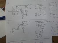
My suggestion/answer for problem (2):
It is best to divide the task in two separate tasks:
* At first calculate the gain without feedback - referenced to the base (base voltage Vb): Ao=Vo/Vb.
Using standard formulas this shouldn`t be a problem.
* Secondly, find the dynamic input resistance r(in) at the base. Don`t forget, that the feedback resistor Rr is drastically reduced due to the MILLER effect.
*
Correction: Get A=Vo/Vs by using the voltage divider rule.
Thus: A=Ao*r(in)/(r(in)+Rs)
 
Last edited:

Circuit 1

Ignoring base currents, we can calculate the quiescent conditions as follows:

  1. R1 and R2 divide the supply voltage in half, so Q1's base is at 5V.
  2. Vbe = 0.6V, so Q1's emitter is at 4.4V
  3. The current through R5 = 4.4V / 5K = 0.88mA.
  4. The voltage across R3 = Vbe of Q2 = 0.6V so the current flowing through R3 and Q1 = 0.6V / 2K = 0.3mA.
  5. The voltage across R4 = Vbe of Q3 = 0.6V so the current flowing through R4 and Q2 = 0.6V / 2K = 0.3mA.
  6. The current through R5 = current through Q1 + current through R4 + current through Q3. From 3, 4 and 5 above, we have 3 of those values, so the current through Q3 = 0.88mA - 0.3mA - 0.3mA = 0.28mA
  7. The voltage across R6 = 0.28mA * 3K = 0.84V so the voltage at Q3's collector = 10V - 0.84V = 9.16V.

Input impedance:

  • The input impedance of the amplifier is equal to the parallel combination of R1, R2 and the input impedance of Q1.
  • The input impedance of Q1 is equal to it's dynamic emitter impedance multiplied by it's current gain.
  • The dynamic emitter impedance (in Ohms) = approximately 25 / emitter current (in mA).
  • So:
    Re(Q1) = 25 / 0.3 = 83.3 Ohms
    Rin(Q1) = 100 * 83.3 = 8.33K
    Input impedance of amplifier = 50K || 50K || 8.33K = 6.25K

Output impedance:

The output impedance equals the parallel combination of R6 and the collector impedance of Q3. The collector impedance depends on what transistor is used but hopefully it will be much greater than R6, so output impedance = almost 3K.

Voltage gain:

  • Voltage gain
    = transconductance of 1'st stage
    * current gain of 2'nd stage
    * current gain of 3'rd stage
    * load resistance (i.e. R6)
  • First stage:
    Re(Q1) = 25 / 0.3 = 83.3 Ohms, so transconductance = 1 / 83.3 = 0.012
    In other words, if the input signal voltage at Q1's base is 1mV then the output signal current from Q1's collector = 0.012mA.
  • Second stage:
    Q2's current gain is 100 but only part of the signal current from Q1's collector goes into Q2's base. The rest goes into R3.
    The fraction that goes into Q2's base = R3 / (R3 + Rin(Q2).
    Re(Q2) = 25 / 0.3mA = 83.3 Ohms
    Rin(Q2) = 100 * 83.3 = 8.33K
    Fraction = 2K / (2K + 8.33K) = 0.1935
    Current gain = 100 * 0.1935 = 19.35
  • Third stage:
    Similar calculation to 2'nd stage:
    Re(Q3) = 25 / 0.28mA = 89.3 Ohms
    Rin(Q3) = 100 * 89.3 = 8.93K
    Fraction = 2K / (2K + 8.93K) = 0.183
    Current gain = 100 * 0.183 = 18.3
  • Voltage gain = 0.012 * 19.35* 18.3 * 3K = 12700


After typing all that, I hit "submit" and got a server error.
Lucky I saved a copy first or I would not be happy right now.
;-)
 

Status
Not open for further replies.

Part and Inventory Search

Welcome to EDABoard.com

Sponsor

Back
Top