Continue to Site

Welcome to EDAboard.com

Welcome to our site! EDAboard.com is an international Electronics Discussion Forum focused on EDA software, circuits, schematics, books, theory, papers, asic, pld, 8051, DSP, Network, RF, Analog Design, PCB, Service Manuals... and a whole lot more! To participate you need to register. Registration is free. Click here to register now.

opamp architecture for large capacitive load ??

Status
Not open for further replies.

cmos_ajay

Full Member level 2
Full Member level 2
Joined
Jan 30, 2007
Messages
126
Helped
0
Reputation
0
Reaction score
0
Trophy points
1,296
Activity points
2,247
Hello,
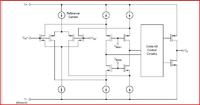
Attached is a picture of a opamp schematic.
It represents TEXAS Instruments op-amp OPA350 as seen in datasheet.

This opamp drives very high capacitive loads ( micro farads ) when connected as a unity gain buffer. It has gain > 100dB . The first stage is a standard folded cascode.
a] What do you think is the architecture of the class AB control circuitry seen in the picture ??
b] To drive high capacitive loads, the miller compensation will 'not' be useful at all
c] Is there any other opamp architecture to drive large capacitive load with high gain and bandwidth ??

Thanks.
 

Attachments

  • OPA350_TI_opamp.JPG
    OPA350_TI_opamp.JPG
    39.9 KB · Views: 203

I don't know about the class AB control circuitry, but I would say it does use Miller compensation.

Most common opamps have a voltage gain stage with Miller compensation, followed by a unity gain buffer as the output stage.

This circuit has a common-source output stage, so the output stage is the voltage gain stage, and Miller compensation is provided by the drain-gate capacitance of the output devices.

This is probably what allows it to be stable with capacitive loads. A simple gain stage with Miller compensation has an output impedance which reduces with increasing frequency (ideal for driving capacitive loads). However, when a unity gain buffer is added at the output this advantage is lost because the buffer's current gain will reduce with increasing frequency.
 

The usual way to achieve stability with high capacitive load is a current source output respectively sufficient high real output impedance and the load capacitor forming the dominant pole.

The OPA350 datasheet states a 1k low frequency output resistance, which is high compared to usual OPs with output buffer. I guess, miller compensation is in effect at zero to low capacitive load. Above a certain load capacitance the output pole becomes dominant.
 

Hello FVM , I could not understand the statement "datasheet states a 1k low frequency output resistance, which is high compared to usual OPs with output buffer. I guess, miller compensation is in effect at zero to low capacitive load. Above a certain load capacitance the output pole becomes dominant."
On page 5 of the datasheet, it says the RL = 1Kohm and the frequency response plot is seen. Can you please clarify your statement ??
Thanks.
 

Which part of the statement is unclear to you?

I was referring to OP output impedance, not load resistance. There's is a singular 1k specification in the text under "Output Impedance". Please review.

Besides this number, the datasheet doesn't specify much, e.g. output impedance versus frequency or open loop response versus load capacitance would be interesting. The overshoot versus load capacitance is the only other information that shines a light on device behaviour.
 

Hello FVM, In my case I am using a folded cascode with class AB stage at the output. I removed the internal miller compensation. Due to the large load capacitor (CL) at the output, the dominant pole is established by the Rout and CL. In the frequency response plot, I see 2nd pole below the F_unity frequency. This gives an almost zero phase margin. To stabilize the amplifier, I can add a Resistor in series with the load capacitor. This gives rise to a left half plane Zero near the 2nd pole and enables phase lead compensation giving a better phase margin. However the position of this zero varies with process, voltage and temperature.
** will you suggest any suitable architecture of opamp (with high gain) that can drive high capacitive load ?
 

  • In 1979 DAMN FAST meant 6000 volts/micro second for unity gain stable buffers.
  • consider history on Comlinear, CLC111, then obsolete National, now an TI LH0021 0.2A consider 1 Amp part **broken link removed**

How many Amps do you need? =C * dv/dt
What driver impedance ? what load impedance ?
What load back EMF?
How good is your layout for parasitics?

TONY
p.s. class AB control circuitry

I suspect patented ( public) current controlled temperature compensated crossover biasing for complementary outputs.
 

In the frequency response plot, I see 2nd pole below the F_unity frequency. This gives an almost zero phase margin.
The question is where the second pole is located? If you can't remove it, reducing gm is probably the easiest way to get a stable feedback loop.
 

ah ok. I was responding to original questions...
  • What do you think is the architecture of the class AB control circuitry seen in the picture ??
  • To drive high capacitive loads, the miller compensation will 'not' be useful at all
  • Is there any other opamp architecture to drive large capacitive load with high gain and bandwidth ?

good answer BTW on Poles. I wonder if it applies to czechs ;)
 

  • What do you think is the architecture of the class AB control circuitry seen in the picture ??

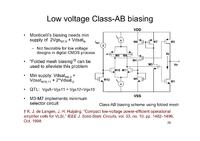
I think for this schematic the folded mesh biasing scheme would be most appropriate
**broken link removed**
 
Hello Erikl, Thanks for the suggestion. I have the paper which gives more information about the circuit. I am also investigating techniques mentioned in AN884 "Driving capacitive loads with opamps" - Microchip Technology
I will post when I see the correct result.
 

Hello FvM, The second pole is located about a decade below the unity-gain frequency. Which gm do I reduce ......gm of stage 1 or stage 2 ??
 

"Where located" meant: which capacitance is representing the pole?
 

Hello, I noticed that after I remove my internal compensation in the opamp and have a large load cap. of 10uF...... there are 2 poles. The first pole is due to the large load capacitor and the output resistance of the opamp. The second pole ( at higher frequency ) is most likely due to the stage 1 output impedance and the stage 1 node capacitance. The position of first pole varies quite a lot with change in load capacitance , but the position of second pole remains almost same.
One option that I think of is to cancel the second pole and use a phase lead network. Another is called 'In the loop compensation technique'
Reading documents : 1) Practical techniques to avoid Instability due to capacitive loading.
2) Chapter 7 'Voltage feedback opamp compensation ' Ron Mancini
 

The architecture of the TI opamp (OPA350 ) shows a 'differential' output taken from the left and right branch and fed to the class AB control. Does this offer some specific advantage ?? Does it avoid the need for Miller compensation between 2 stages ? Will there will be only one pole due to the class AB output stage ??
 

I think it depends on the class AB control stage implementation: if this stage also has gain > 1 , you have a 3-stage amp, and you'll probably need a nested miller compensation (NMC) scheme, see e.g. Compensation of Class-AB drivers in the above mentioned tutorial (pp. 31 ff).
 
Status
Not open for further replies.

Part and Inventory Search

Welcome to EDABoard.com

Sponsor

Back
Top