Continue to Site

Welcome to EDAboard.com

Welcome to our site! EDAboard.com is an international Electronics Discussion Forum focused on EDA software, circuits, schematics, books, theory, papers, asic, pld, 8051, DSP, Network, RF, Analog Design, PCB, Service Manuals... and a whole lot more! To participate you need to register. Registration is free. Click here to register now.

Large signal CE amplifier

Status
Not open for further replies.

goldsmith

Advanced Member level 6
Joined
Dec 14, 2010
Messages
3,981
Helped
741
Reputation
1,486
Reaction score
726
Trophy points
1,413
Location
Tehran - IRAN
Activity points
24,546
Hello my friends!
I know that the ce amplifiers are small signal . but i designed an amplifier ( ce) for small signal , then with changing(random) values of R1 and R2 , i could amplify a 5 volt signal to 11.5 volt as well as . what happened? i wanna find a formula for designing an ce or cb or cc (in class A) for large signal and i don't want to changing the values (random) . i want to calculate the best values for large signal . is here any experience or suggestion? is it possible that you guide me , please?
Thanks In Advance
Goldsmith
 

My understanding of large signal is, that linear approximations of transistor characteristic no longer apply. For an exact calculation, you have to refer to exponential (Shockley) equations.
 

Thanks for your reply but how is its design with equations that you said?
Thanks
 

but how is its design with equations that you said?
You didn't tell an exact design problem.

The exponential characteristic applies to instantaneous values, not averaged voltages or currents. It depends on the problem, if you can derive menaingful average values, e.g to set a bias point.
 

If you want large signal swing we simply use op-amp or we use two ore three stage BJT amplifiers with negative feedback.
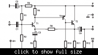
Here you have a classic example of such an amplifier


As for the single stage to get maximum voltage swing we need a lot of voltage headroom from power supply.
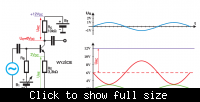
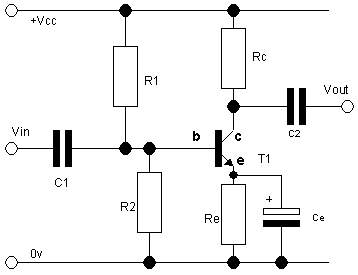
Try to analysis this for example


Vcc = 12V; Vc = 6V (red plot ); Ve = 2V (green plot) ; Vinput = 1V (blue plot).


And theoretical the optimal Vce without Ce capacitor:

\[Vce_{opt} = Vcc*\frac{Rc+Re }{2(Rc+Re)}\approx 0.5*Vcc\]
And
\[Ic_{opt}=\frac{Vcc-Vce(sat)}{2(Rc+Re)}\]

And if we add a Ce capacitor we get:

\[Vce_{opt}= Vcc*\frac{Rc}{2Rc+Re}\]
And
\[Ic_{opt}=\frac{Vcc-Vce(sat)}{2Rc+Re}\]


When we design single stage BJT amp we use this formulas

Re = 0.1...0.3 * Vcc/Ic or we set Ve >> Vbe usually 1V or more.

Vce > V_output_max_peak + Vce(sat_max) + V_headroom

V_headroom - safety margin typical 20% of V_out_max

Ic = V_output_max_peak / ( RL * safety margin)


\[Rc=(\frac{(Vcc - Ve - Vce)*0.8}{Voutmax}-1)*RL\]

Or sometimes

Rc = ( Vcc - Ve - Vce) / Ic

Rload ≧10*Rc

And for the voltage divider

R1 = (Vcc - Vb) / (11*Ib);

R2 = Vb / (10*Ib)


Vb = Ve + Vbe

33_1320251554.png


But as usual in electronics there is no simply rule which take into account all factors that the designer must consider when tries to meet the design specification. And the key word here is compromise.
 
For example i want to design a ce amplifier with RI = 10 k ohms and RO = 1k ohms and AV = 5 ( and my input voltage is large for example 7 volts).
Appreciate

---------- Post added at 20:22 ---------- Previous post was at 20:17 ----------

I'm professional in designing the multistage class A small signal amplifier but large signal is difficult , i think.
 

For example i want to design a ce amplifier with RI = 10 k ohms and RO = 1k ohms and AV = 5 ( and my input voltage is large for example 7 volts).
Well, for specification that you give is it clear why we don't use a single stage BJT amp.
Your Ro is too low for CE amplifier and the output voltage swing more then 35V? This must be a joke.
 

The circuits suggested by jony130 try to operate the transistors still in an (almost) linear range. Calculations are also based on assumption of linearity. In this case, there's no large signal aspect involved, I think. The problem is just about selecting a topology that allows sufficient voltage swing and uses negative feedback to get linear behaviour.

Particularly the three transistor circuit is a good starting point.
 

I just wanna use from one stage as a large signal . for example i wanna give 7 to it and get that AV.
 

Goldsmith can you tell my what is the difference between small signal and large signal?

Do you want distorted output signal? Or maybe you want linear (not distorted signal)?
 

Dear jony130
Hi
What do you mean? it is clear that what is the difference between large signal and small signal. i know that we can design small signal amplifier without distortion and we can design large signal without distortion too. i changed the values of resistances of ce amp(small signal ) (randomly) and changed may amp to the large signal amp. as well as. i know that in large signal we can not use hybrid model and we have to use an eberes mole model! guide me in ebers mole model designing , please.
Best Regards
Goldsmith
 

Simply use the same equations for large signal design as you use for small signal.
 
  • Like
Reactions: FvM

    FvM

    Points: 2
    Helpful Answer Positive Rating
Dear Friend!
Again Hi
It is completely wrong! because the behavior of the transistor at large signal is magically nonlinear! and it will be logarithmic .
And my problem is that i want to design a nonlinear class a amplifier! . if you design an small signal amplifier , as you said , if your input signal become large , your out put THD will increase as high as !
Thanks for your reply
Goldsmith
 

The approach suggested by jony130, which is also demonstrated by the three-transistor amplifier is to use circuits, where the non-linearity of the transistor characteristic doesn't take effect, respectively is reduced to an acceptable amount.

With suitable circuits, the claimed method comes true:
Simply use the same equations for large signal design as you use for small signal.
 

The key to getting large voltage swings is to drive the transistor so its CE resistance swings between (a) high impedance and (b) lowest possible 'on' resistance (saturation).

To facilitate this, related components must be sufficiently low resistance.

Disadvantage: Non-linear action when your waveform gets close to supply rails. Because at the trough the transistor is no longer operating in its linear region. Or at the crest the output will get flattened by running into the supply rail.

So a sinewave turns into this (ocean waves).

**broken link removed**

This is distortion although it may continue to sound smooth.
 
Last edited:

Dear BradtheRad
Again Hi
Thanks for your reply.
But when we wanna amplify each signal ( large signal) we can control its THD ratio as well as. i told in top posts that when i changed the values of resistances randomly , i obtained my desired aim but i want to find an standard way for its calculation. If you help me to find its calculation i will appreciate you. I know that these types of amplifiers are not useful currently and i'm professional to designing the new methods of amplifiers such as class D or E or F ore etc . but i want to learn each thing in electronics! I hope that you help me.
With appreciate
Goldsmith
 

we can control its THD ratio as well as
You can't control it at will. You can optimize the bias point of a single stage CE amplifier, drive it with a current rather than a voltage signal, but the "secret" of achieving high linearity with large signal is plenty of redundant gain and negative feedback. That's what e.g. high quality analog audio circuits do since 50 years. A single stage CE amplifier won't get rid of it's THD if you demand large signal and some gain from it.
 

Dear FvM
Hi
Thanks for your reply.
But you said that we can do it with nonlinearity schokley equations! and i want to know that how we can design with those equations? and as i said with one stage when i changed the value of resistance randomly , its achieved.
Thanks in advance
Goldsmith
 

The Shockley equation allows to predict the non-linearity or exactly calculate a bias point, but it can't cancel the non-linearity in most cases. There are a few exceptions. e.g. a current mirror, that can be utilized as a linear current amplifier, or a Gilbert cell multiplier. But is doesn't help to reduce the distortion of a trivial CE stage used as a voltage amplifier.
 

Dear FvM
I need to ask an important question! why when i changed the value of resistances (randomly) i obtained my aim? if you want i can put here my values.
Respect
 

Status
Not open for further replies.

Part and Inventory Search

Welcome to EDABoard.com

Sponsor

Back
Top