Continue to Site

Welcome to EDAboard.com

Welcome to our site! EDAboard.com is an international Electronics Discussion Forum focused on EDA software, circuits, schematics, books, theory, papers, asic, pld, 8051, DSP, Network, RF, Analog Design, PCB, Service Manuals... and a whole lot more! To participate you need to register. Registration is free. Click here to register now.

PA phase shift changing with amplitude

Status
Not open for further replies.

mtwieg

Advanced Member level 6
Joined
Jan 20, 2011
Messages
3,903
Helped
1,311
Reputation
2,628
Reaction score
1,435
Trophy points
1,393
Activity points
29,979
Hello, I've built a a 64MHz 4W class A PA for use in a MRI system, and I've recently discovered that its phase shift changes depending on the input and output power, by about 30 degrees over its full range. This is frustrating, because I need to vary amplitude and phase on the output with a good degree of accuracy. To be specific, I'm making short RF bursts which generally differ by 6dB in power, and must be 90 degrees out of phase. I have a feeling that this is a problem that linear amplifiers will always have to some degree. So I'm considering making a class D current fed amp, which would be amplitude modulated by its drain voltage. Would a switching amp have less phase variation than linear amps?

Also, I'd like to have a way to measure the phase between two RF pulses, but I'm not sure how. I have a nice oscilloscope, but using its cursors seems like a sloppy method. I also have a good signal analyzer, but I don't how I could possible use it to measure relative phase. Any advice?
 

A switching amp will have more phase variation than a linear one.
Usually if the linear PA is designed for a single frequency, and if it use a well designed bias circuit (filtering, bias point, temperature compensation, etc), should be no problem to meet the AM-PM requirements.
 
  • Like
Reactions: mtwieg

    mtwieg

    Points: 2
    Helpful Answer Positive Rating
A switching amp will have more phase variation than a linear one.
Really? Why is that? If I use drain modulation, then I assume that the only phase shift would be due to changing output impedance as Vd changes. But if I use a class D amp with a low Q output tuning network, I assumed that the changes would be pretty much negligible. And since the input is hard switching, I shouldn't have to worry about input capacitance variations.
Usually if the linear PA is designed for a single frequency, and if it use a well designed bias circuit (filtering, bias point, temperature compensation, etc), should be no problem to meet the AM-PM requirements.
I know it's not temperature that's causing it. Must be something with the biasing. Would a fixed gate bias voltage work, or would it be necessary to regulate the Iq with feedback?
 

Theoretically class-D (or other switching classes) are fine, but in reality is no amplifier can be a true Class-D, as non-zero switch resistances and capacitive as well as inductive parasitics restrict the ideal performances, when a linear (class-A) PA stays (luckily) in the same state from the begging to the end.

Filtering and impedances at low frequencies (baseband) are very important for the bias circuit to get good AM-PM.

I don't know if is the case, but there is a type of thermal memory effect that can generate poor AM-PM performance. This is related to the fast changing of the temperature of the junctions (with modulation), which is hard to be detected with standard temperature measurements.
 
This is a very common problem in communications systems. It is called AM-to-PM conversion, and amplifiers are specified to minimize it.

I would suggest that you use a very stiff (low impedance) bias structure to keep any RF rectification to a minimum. A DC bias point change will cause a phase shift.

Another reason for a phase shift would be the generation of harmonics and/or clipping, which, when summed in the time domain, can look like phase shift. You might actually want to use a technique called "feed fortward" design, where a power amp supplies most of the output power, but a second parallel amp supplies the sine wave peaks. The combination of the two is a reconstructed pure sine wave, without the phase shifts you are experiencing.

Rich
 
Last edited by a moderator:
mtwieg: In case of a real class A amp (so a good heat generating device), and modern LDMOS devices, 30 degrees seems a lot to me. I assume that the supply current doesn't change much during the pulse.

If it does change, can you repeat the measurements with almost CW? Just to exclude any bias change due to changing supply current through chokes.

regarding the class D, I think the problem is in the drive signal feed through. When you reduce the output by reducing the drain voltage, the feed through signal (via the reverse capacitance) will no longer be small w.r.t. the output, hence affecting phase and amplitude.
 
  • Like
Reactions: mtwieg

    mtwieg

    Points: 2
    Helpful Answer Positive Rating
This is a very common problem in communications systems. It is called AM-to-PM conversion, and amplifiers are specified to minimize it.

I would suggest that you use a very stiff (low impedance) bias structure to keep any RF rectification to a minimum. A DC bias point change will cause a phase shift.
Now that you mention it, my bias structure impedance may be high (what would you define as a suitable impedance at DC for biasing?). I'm biasing my gate through about 300ohms and a 2.2uH inductance. But I have trouble seeing how that impedance can hurt me. The only DC path to my gate should be from my bias circuit (I'm using a MRF173 FET). So how could the operation of the FET change my gate bias?
Another reason for a phase shift would be the generation of harmonics and/or clipping, which, when summed in the time domain, can look like phase shift.
I measured my phase shift by putting a tuned coil on the output of the amp and looking at the field from the coil with a pickup loop. The coil has a Q of about 150, so it filters off pretty much all harmonics, so I doubt this is the case.

mtwieg: In case of a real class A amp (so a good heat generating device), and modern LDMOS devices, 30 degrees seems a lot to me. I assume that the supply current doesn't change much during the pulse.
I only turn on the bias when doing a pulse (which is only about 50us long). So I wouldn't notice current draw changes in that case.
regarding the class D, I think the problem is in the drive signal feed through. When you reduce the output by reducing the drain voltage, the feed through signal (via the reverse capacitance) will no longer be small w.r.t. the output, hence affecting phase and amplitude.
Yes this is a very good point. I was planning on using devices with as small of a Cdg ass possible (which I assume is the primary mechanism for feed through), but I would definitely have to watch out for this effect.

Theoretically class-D (or other switching classes) are fine, but in reality is no amplifier can be a true Class-D, as non-zero switch resistances and capacitive as well as inductive parasitics restrict the ideal performances, when a linear (class-A) PA stays (luckily) in the same state from the begging to the end.
Right, everything is nonideal, but it's just a matter of which is closer to ideal. Probably no use in trying to generalize between two so drastically different topologies...
Filtering and impedances at low frequencies (baseband) are very important for the bias circuit to get good AM-PM.
Again, this may be my issue. But what is the actual mechanism here that causes poor AM-PM? And what impedance should be aiming for?
I don't know if is the case, but there is a type of thermal memory effect that can generate poor AM-PM performance. This is related to the fast changing of the temperature of the junctions (with modulation), which is hard to be detected with standard temperature measurements.
Right, thermal memory is one thing I probably won't be able to model or compensate for... which is why I thought class D might be a better choice since it should dissipate less heat.

Thanks all for the replies, this is all very useful for me.
 

Regarding bias, How did you bias the drain? When you turn on the gate bias, it takes time for the drain bias to settle. Are you sure everything has been settled before applying the RF input power?

Did you match the output for maximum power at a certain drive level (with the risk of operation close to voltage saturation and effect of non-linear mosfet capacitances), or did you accept some reduction in gain to assure you stay away from saturation/clipping?

What is the DC input power when generating 4 W. I hope it is huge, so you are in fact having a "small signal" amplifier.
 
  • Like
Reactions: mtwieg

    mtwieg

    Points: 2
    Helpful Answer Positive Rating
The impedance at low frequencies this should be low, but ideally would be to tune the filter circuit for best performance that you are looking for.

Was happened to me to have poor AM-PM in a multistage PA and the reason was the input match of the driver, which was changing dynamically with input power. Just made the bandwidth of the match wider and problem was solved.
 
  • Like
Reactions: mtwieg

    mtwieg

    Points: 2
    Helpful Answer Positive Rating
I measured my phase shift by putting a tuned coil on the output of the amp and looking at the field from the coil with a pickup loop. The coil has a Q of about 150, so it filters off pretty much all harmonics, so I doubt this is the case.
To get considerable phase modulation, as you reported, there must be some high Q circuit part that slightly changes it's resonance frequency depending on the signal level. When I hear about your test setup, I suspect, that the tuned coil added for test is the cause of phase modulation. If you don't have other high Q resonant circuits in the PA, it's the most likely explanation, I think. The resonance frequency shift can be e.g achieved by signal dependent output impedance variations.

As a first try, get rid of the additional filter.
 
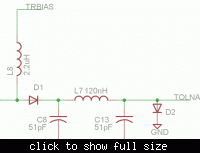
Here's a schematic of what I have at the moment:
TXschematic.png
Regarding bias, How did you bias the drain? When you turn on the gate bias, it takes time for the drain bias to settle. Are you sure everything has been settled before applying the RF input power?
The drain is biased as shown. The drain voltage is a fixed 30VDC (this amp is input modulated, not gate or drain modulated). I allow the gate bias 20us of rise time, then switch the TR switch on, wait 4us more, and then apply the RF input. These should allow plenty of time for both stages to reach a steady state. I check this by looking at the source current (using the source resistors), the drain voltage, and the voltage at the anode of D1. And I measure the phase about 20us into the RF pulse. Everything should be steady by then...
Did you match the output for maximum power at a certain drive level (with the risk of operation close to voltage saturation and effect of non-linear mosfet capacitances), or did you accept some reduction in gain to assure you stay away from saturation/clipping?
As shown in the schematic, there isn't any impedance matching done anywhere. Previously I did have impedance matching, but I ran into a problem where the gain of the transmitter was drifting with temperature (I had a thread on that a while back...) and I found that removing the matching networks helped a lot. Now the gain deviates by about 0.1dB. But I don't think I need it that good, so if adding a matching network back in would help, I'd definitely consider it.
What is the DC input power when generating 4 W. I hope it is huge, so you are in fact having a "small signal" amplifier.
Currently I'm biasing the first stage with 0.35A and the second stage with 0.81A. Strangely, I still start to see significant distortion on the output, despite the huge bias I'm applying.

The impedance at low frequencies this should be low, but ideally would be to tune the filter circuit for best performance that you are looking for.
In the MRF173 datasheet, they show the gate bias being applied through a 10K resistor... I guess they don't care about stiff biasing or something.

Was happened to me to have poor AM-PM in a multistage PA and the reason was the input match of the driver, which was changing dynamically with input power. Just made the bandwidth of the match wider and problem was solved.[/QUOTE]I've looked at wideband input matching techniques before (mainly in this application note **broken link removed**), but saw them as unnecessary and intimidatingly complicated. Should I try going for a three reactance network as described in that document?

To get considerable phase modulation, as you reported, there must be some high Q circuit part that slightly changes it's resonance frequency depending on the signal level. When I hear about your test setup, I suspect, that the tuned coil added for test is the cause of phase modulation. If you don't have other high Q resonant circuits in the PA, it's the most likely explanation, I think. The resonance frequency shift can be e.g achieved by signal dependent output impedance variations.

As a first try, get rid of the additional filter.
This is a reasonable explanation, but without a high Q filter on the output I don't see how I could measure the phase of the fundamental signal accurately at high power levels. I have a nice VNA, which has a power sweep option on its menu, but I haven't been able to get it to work for some reason... that would be so useful for this...
 
Last edited:

Also I still want to get some mathematical understanding of how AM-PM occurs. The only source I could find with a quantitative analysis was this: **broken link removed**
It makes sense somewhat... the odd harmonics resulting from compression will result in a DC component on the output. If the amplitude is changing continuously, then the resulting DC does as well, causing the zero crossings of the output to change, and thus giving phase shift. However, this only applies to when the input signal is continuously changing amplitude. If the amplitude is changed, but then left constant for a while, and the DC component is filtered off, then the output should settle to the original phase shift, right?... so this really doesn't explain AM-PM conversion in the sense that different amplitudes have different phase shifts at steady state; just that rapidly modulating amplitude will cause apparent phase modulation. Does this sound right?
 

but without a high Q filter on the output I don't see how I could measure the phase of the fundamental signal accurately at high power levels
The filter should have sufficient harmonic suppresion, and preferably no phase or amplitude dispersion near the carrier frequency. That seems feasible. In addition, you should check, that you don't have unwanted resonances with respective phase dispersion created by the chokes. This would be seen from the amplifier S21.

I also wonder about the purpose of D1/D2. Do you operate it as an attenuator? In any case, it will make the low-pass filter characteristics strongly ampltitude depending, related to both attenuator setpoint and amplifier output power.
 
The filter should have sufficient harmonic suppresion, and preferably no phase or amplitude dispersion near the carrier frequency. That seems feasible.
Okay, I could probably make a 3 pole butterworth LPF. That should be good, right?
In addition, you should check, that you don't have unwanted resonances with respective phase dispersion created by the chokes. This would be seen from the amplifier S21.
The chokes are air core, and should be resonant in the hundreds of MHz. Also, what is phase dispersion?
I also wonder about the purpose of D1/D2. Do you operate it as an attenuator? In any case, it will make the low-pass filter characteristics strongly ampltitude depending, related to both attenuator setpoint and amplifier output power.
Oh yeah, I forgot to mention that's my TR switch. The 50ohm matched coil connects to the cathode of D1. I thought I'd throw it in just in case it's part of the problem.
 
Last edited:

With phase dispersion, I mean dφ/dω, phase versus frequency variation. With high choke self resonance frequencies, it should be no problem.

It's basically the same with the output filter. If the S21 is almost constant around the frequency of interest, the amplitude sensitivity can be expected low as well. A butterwoth filter shouldn't be bad.

I don't exactly understand the TR switch configuration, particularly D2. Did you replace it by short/open for the measurement?
 
Regarding Drain bias, I agree, this can't be the problem given the time available to get steady state.

the output stage:
Ignoring increase of drain voltage due to resonance at harmonics, 4 W into 50 Ohms would result in 20Vp drain voltage swing, so this shouldn't result in drain voltage clipping.

There can be a current clipping problem, 4W into 50 Ohms is about 0.4 A, however this device has 105 pF output capacitance and 10 pF reverse (115 pF total). This is 22 Ohms, resulting in a reactive current of about 20/22 = 0.92A. Total AC current as seen by Gm current source will be about 1Apk. If you don't compensate this capacitance with an inductance, the amplifier will leave class A operation (as you have 0.81A bias current). You may see a slight current increase from steady state during the RF pulse.

The output capacitance is also voltage dependent (as shown in the datasheet), so this will introduce phase shift between the actual current through Gm and the drain voltage at increasing RF drain voltage. It is like the effective capacitance increases with increasing RF drain voltage. A smaller or UHF device has less output (and input) capacitance.

You may also check the first stage for voltage or current clipping. If you have a fast oscilloscope that can display sufficient harmonics, you may check the waveforms (you probably already did as you mentioned output distortion).

The 30 degrees phase shift, is this for the complete amplifier, or for one of the stages?

Regarding the actual amplifier load (the 50 Ohms tuned coil), this may suppress harmonics towards the output, but this doesn’t guarantee that there are no harmonics at the drain. As you mentioned distortion, they may be present.
 
  • Like
Reactions: mtwieg and FvM

    FvM

    Points: 2
    Helpful Answer Positive Rating

    mtwieg

    Points: 2
    Helpful Answer Positive Rating
With phase dispersion, I mean dφ/dω, phase versus frequency variation. With high choke self resonance frequencies, it should be no problem.

It's basically the same with the output filter. If the S21 is almost constant around the frequency of interest, the amplitude sensitivity can be expected low as well. A butterwoth filter shouldn't be bad.
okay makes sense.
I don't exactly understand the TR switch configuration, particularly D2. Did you replace it by short/open for the measurement?
It's a very common SPDT switch configuration using PIN diodes and a lumped element lambda/4 transmission line. Figure 2 in this doc: https://www.skyworksinc.com/downloads/press_room/published_articles/Elektronica_072009_English.pdf

There can be a current clipping problem, 4W into 50 Ohms is about 0.4 A, however this device has 105 pF output capacitance and 10 pF reverse (115 pF total). This is 22 Ohms, resulting in a reactive current of about 20/22 = 0.92A. Total AC current as seen by Gm current source will be about 1Apk. If you don't compensate this capacitance with an inductance, the amplifier will leave class A operation (as you have 0.81A bias current). You may see a slight current increase from steady state during the RF pulse.
Good observation... will a conjugate match on my drain to my 50ohm load provide nulling of this current, or do I need to hang an inductor in parallel with my Cds (with DC blocking caps of course) somehow?
The output capacitance is also voltage dependent (as shown in the datasheet), so this will introduce phase shift between the actual current through Gm and the drain voltage at increasing RF drain voltage. It is like the effective capacitance increases with increasing RF drain voltage. A smaller or UHF device has less output (and input) capacitance.
I thought capacitance would decrease with increasing voltage? Anyways yeah a different device may help a lot, but I'd like to make this a learning experience rather than just playing trial and error with different parts.
You may also check the first stage for voltage or current clipping. If you have a fast oscilloscope that can display sufficient harmonics, you may check the waveforms (you probably already did as you mentioned output distortion).
Yes, I'll check that too. I do have a 500MHz scope, so I should be able to.
The 30 degrees phase shift, is this for the complete amplifier, or for one of the stages?
The whole thing.
Regarding the actual amplifier load (the 50 Ohms tuned coil), this may suppress harmonics towards the output, but this doesn’t guarantee that there are no harmonics at the drain. As you mentioned distortion, they may be present.
Well I should emphasize that the coil is the intended load for the amplifier, so the phase with that load is ultimately what I'm interested in. However for diagnostic purposes, yes I should also be probing drain voltages directly. Also, on a future design I may throw in a small current sense resistor on the source (in series with the source capacitor). Might that be useful for telling whether my distortion is due to lack of bias voltage or current?
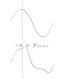
am-pm, uncompressed vs compressed output:

I assume you're saying that distortion makes it look like phase shift? Sure, that's why I was intending to do measurements with a filter on the output.

Also, I was able to get the power sweep function on my VNA to work (only annoying limitation is that it can only sweep 15db at a time). I put the amp on it briefly and was able to see the change in phase shift happen, and it was right around the start of gain compression. This was with just a 40dB broadband attenuator as a load. I'm currently rushing development on a couple other things at the moment (got a grant application coming up!) so I probably won't get any more lab work done on this until next week. But until then, I wanted to know if the VNA power sweep will give an accurate measure of the gain and phase of the fundamental component of the signal, or if I should apply a filter to the output?
 

It's a very common SPDT switch configuration using PIN diodes and a lumped element lambda/4 transmission line.
Unfortunately, all relevant components, except for the diodes are missing in your schematic. Seeing the paper, I get an idea, how the T/R circuit could be connected. To understand possible phase shift issues, we should see the real circuit used in the test. Presently, it looks like a shorted filter output with no antenna feed at all.

 
#Regarding output capacitance and matching.
I would first breakdown the problem (so studying each (amplifier) stage separately).

Adding inductance to ground (as close as possible to the drain) will compensate this current, you may use L4 for that (make sure you use a good bypass capacitor(s) for C10 as it will carry reasonable RF current).

I would not recommend full conjugate match. Though it gives maximum gain, it may lead to slightly voltage-saturated operation.


#Increasing capacitance with increasing RF drain voltage.
You are correct that the output capacitance reduces with increasing DC drain voltage, but for the AC case it is different. The negative half of RF drain voltage experiences an increasing capacitance though the positive half experiences a reducing capacitance. The increase is larger then the decrease, so effectively, the drain capacitance increases somewhat.

In a parallel equivalent circuit, your 50 Ohms is shunted by a voltage dependent –j22 capacitance. Some change in this capacitance will introduce phase shift.

You may transform your 50 Ohms load to a lower value (as seen by the drain). This reduces the effect of the capacitances. This requires more RF current and it may become difficult to maintain class A operation. You may consider class AB operation and find a sweet spot (bias current issue). I know it reduces gain and it requires you to observe the impedance as seen by Gm for higher harmonics as now Id will contain lots of harmonics.

Do you have good familiarity with a simulation package (that allows non-linear simulation)? If so, you may change an existing transistor model (including the non-linear capacitances). It takes time, but in simulation you can turn on and off certain behavior to see the effect on phase versus output power. I learned a lot by doing this for a 100 MHz linear PA with a spice simulator.

To be honest, I don't believe that in your current circuit, the mosfet's voltage dependent output capacitance is the root cause for 30 degrees phase shift change versus power. It introduces a fixed phase shift, but as it is off-resonance, the effect on phase change will be small. It can be a secondary source (as you need to apply more gate drive).


Class D (or other switching scheme).
I reread you original posting again. You mentioned you only need about 6 dB change in power. In that case a switching class amplifier based on some medium power upper UHF ldmos can be an option. You only have to halve the supply voltage to get a 6 dB step. Note that such amplifiers are very load sensitive. Some inconvenient load and yo have to place a new mosfet.

---------- Post added at 17:11 ---------- Previous post was at 17:10 ----------

Unfortunately, all relevant components, except for the diodes are missing in your schematic. Seeing the paper, I get an idea, how the T/R circuit could be connected. To understand possible phase shift issues, we should see the real circuit used in the test. Presently, it looks like a shorted filter output with no antenna feed at all.


I also have problems with this T/R switch, but when it contains quarter wave section not shown in this circuit, it may function.
 
  • Like
Reactions: mtwieg

    mtwieg

    Points: 2
    Helpful Answer Positive Rating
Status
Not open for further replies.

Part and Inventory Search

Welcome to EDABoard.com

Sponsor

Back
Top