Continue to Site

Welcome to EDAboard.com

Welcome to our site! EDAboard.com is an international Electronics Discussion Forum focused on EDA software, circuits, schematics, books, theory, papers, asic, pld, 8051, DSP, Network, RF, Analog Design, PCB, Service Manuals... and a whole lot more! To participate you need to register. Registration is free. Click here to register now.

HFSS lumped port and wave port

Status
Not open for further replies.

myem

Full Member level 2
Full Member level 2
Joined
Dec 12, 2003
Messages
127
Helped
0
Reputation
0
Reaction score
0
Trophy points
1,296
Visit site
Activity points
972
wave port

What is the difference of lump port and wave port ?
If I want to get S-parameter of spiral inductor , what type I should use ?

thanks
 

hfss waveport

Lumped ports:
Lumped ports are similar to traditional wave ports, but can be located internally and have a complex user-defined impedance. Lumped ports compute S-parameters directly at the port.The complex impedance Zs defined for a lumped port serves as the reference impedance of the S-matrix on the lumped port. The impedance Zs has the characteristics of a wave impedance; it is used to determine the strength of a source, such as the modal voltage V and modal current I, through complex power normalization. (The magnitude of the complex power is normalized to 1.) In either case, you would get an identical S-matrix by solving a problem using a complex impedance for a lumped Zs or renormalizing an existing solution to the same complex impedance.
By default, the interface between all 3D objects and the background is a perfect E boundary through which no energy may enter or exit. Wave ports are typically placed on this interface to provide a window that couples the model device to the external world.

Wave ports:
HFSS assumes that each wave port you define is connected to a semi-infinitely long waveguide that has the same cross-section and material properties as the port. When solving for the S-parameters, HFSS assumes that the structure is excited by the natural field patterns (modes) associated with these cross-sections. The 2D field solutions generated for each wave port serve as boundary conditions at those ports for the 3D problem. The final field solution computed must match the 2D field pattern at each port.
HFSS generates a solution by exciting each wave port individually. Each mode incident on a port contains one watt of time-averaged power. Port 1 is excited by a signal of one watt, and the other ports are set to zero watts. After a solution is generated, port 2 is set to one watt, and the other ports to zero watts and so forth.


With lumped ports you should know the characteristic impedance of the connected feeding line for calculating S-matrix, while with wave ports, if correctly sized, portZ0 defines the reference impedance for calculating S parameters, and it automatically takes the value of the Zo impedance of feeding line. If I were you, I would prefer wave ports, always if you are not obliged of defining an internal port.

Regards,

Ivan
 
I got a slight adjustment (at least for HFSS V.11 and 12):

The magnitude of the complex power is normalized to 1.

This is actually not completely true. The real power (real part of the incident power) is normalized to 1W by default. But when using complex (lumped) port impedances, the (total) incident power can be (much) higher, as can be seen by calculating the antenna parameters (via right-click onto the radiation sphere). To avoid this I suggest not using complex impedances but use a real port with normalization onto the complex value (the normalization actually takes compex numbers with either 'i' or 'j', at least in V12) or by using a lumped admittance element with X=Im(Z) after the port with the real impedance part Z_port=Re(Z).
 
Hey KILLERCHAKRAVARTI,
The port sizing guidelines for a microstrip structure is given in HFSS Manual on the 2nd last page. For a microstrip structure, the port dimensions should be:
height = between 6h and 10h
width = 10w (if w>=h)
or 5w (if w<h)
where w is width of trace
h is height(thickness) of substrate
 
the above statement is valid for the waveport, not lumped port. The lumped port for a microstrip should be as wide as the signal line and drop straight the the ground plane. Lumped ports should always contact two conductors.

have fun, :)
 
Dear tallface, Can you please give the reference of your statement? As far as I have seen in the manual, it doesnt say that those port size guidelines are only for waveport.
Thanks
 

Ahsaan, the best reference is to try it ;) But basically, the waveport is a 2D eigen solver and requires a cross section of given transmission line to determine the natural modes of the cross section. The reasoning for the waveport dimensions is due to the fact that the edges of a waveport are seen as PEC boundaries in the 2D Eignesolver. If these edges are too close to the signal line, then you have artificial coupling that will perturb the port impedance, hence the "rules of thumb" for port sizing.

As for lumped ports...

Remember that waveports have PEC boundaries on their edges and solve for the eigenmodes, well lumped ports have PEC boundaries on the edges that contact conductors and PMC boundaries on the edges that do not contact conductors. As you can imagine, this forces a field distribution that allows for uniform current :) (which is the same as saying the fundamental mode of an infinite planar waveguide mode) This is why you simply draw a rectangle that connects one conductor to another. Also be aware that by forcing this excitation, you must provide the reference impedance while the waveport will solve for the port impedance and use the dispersive impedance as a generalized reference for generalized S matrices.

Have Fun ;)
 
Back to KILLERCHAKRAVARTI's question: I would not recommend using a lumped port for a microstrip patch antenna anyway. I would use a coax port (meaning a coax connector model using a waveport) - that way you can assume that in the end, once you actually build and measure your antenna, you will get well agreeing results. In my experience, this is always the best choice (although the solving time is slightly increased compared to the lumped port model).
 

Re: hfss waveport

Lumped ports:
………………………………

Ivan

Could you please tell me how to deal whit message below:
Port refinement, process hf3d error: Port 1 does not have a solved inside material on either side..
As a new comer to HFSS ,I have tried to save this problem some times by myself ,but never get the right answer.
And could you please tell what's the difference between "Do Not Renormalize" and "Renormalize All Modes Full Port Impedance".
Thanks so much..
 

Generally, bodies made of metals are not solved on the inside, because normally you dont care about that. The waveport however needs something to be solved inside on one of its sides -- otherwise it would not make sense anyway. So, have a look at your port and the materials on its sides. For example, if you want to make a coax model, then the one side is usually a PEC disc (not solved inside) while the other has the middle pin of the coax and also the isolator material (e.g. Teflon in practice) which is solved inside. Or sometimes the waveport lies on the (radiation) boundary of your model, then of course one side is not solved (because it is the outside of your model) but the other is usually vacuum, which of course is solved inside.

...if that did not help, maybe you should upload your model.

As to the renormalization: the lumped port requires you to give a port impedance, like 50 ohms, but after everything has been solved, you can still look how it would be if you were looking at your model e.g. through a 75 ohm feed by renormalizing everything (I'm sure you can find the actual math in the help) to that impedance. If it is a waveport, it will find its own impedance (so you should check that that impedance actually makes sense for your simulation), and then again, you can renormalize to whatever you want to actually look at.
 
That doesn't look quite right to me... but it's hard to say, from those pictures.
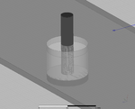
coax1.png
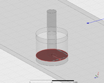
coax2.png
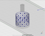
coax3.png
The first shows the coax stub in general. The second shows the waveport, applied to the inner face of the coax end cylinder (or rather disk). And the third the outer conductor, which I usually model by just applying PerfE boundary to the outer lateral surface of the isolation material cylinder (usually Teflon).
 

I tried as you said last night,and I felt that I get the right way to set a wave port .
Thanks very much.
 
Re: hfss waveport

hi Ivan
could you tell me ,

I have designed a square MSA with dual probe feed.But im unable to see E plane & H plane plots for cross & co polarization, I am using HFSS v11. could u tell me 1)where should i see its results ? to see this should i apply excitation to each probe by creating 3 design 1-both probe ,2-1stprobe,3-2nd probe excitation?
2)How to decide its circular or linear polarization?
3) what are the values of theta & phi to see this polarization?
Please reply as early as possible


Thanking you in Anticipation.
 

Status
Not open for further replies.

Part and Inventory Search

Welcome to EDABoard.com

Sponsor

Back
Top