Continue to Site

Welcome to EDAboard.com

Welcome to our site! EDAboard.com is an international Electronics Discussion Forum focused on EDA software, circuits, schematics, books, theory, papers, asic, pld, 8051, DSP, Network, RF, Analog Design, PCB, Service Manuals... and a whole lot more! To participate you need to register. Registration is free. Click here to register now.

0-30V, 0-7A Adjustable Switching Power Supply

Status
Not open for further replies.

Hesambook

Full Member level 2
Full Member level 2
Joined
Sep 26, 2007
Messages
130
Helped
1
Reputation
4
Reaction score
10
Trophy points
1,298
Activity points
3,165
DC to DC buck converters is a famous topology in the electronic and a widely used circuit in electronic devices. A buck converter steps down the input voltage while it increases the output current. In this article/video, I have discussed a DC to DC buck converter that can be used effectively as a switching power supply. The output voltage and current are adjustable: 1.25V to 30V and 10mA to 6A (continuous). The power supply supports the constant voltage (CV) and constant current (CC) features. Two LEDs demonstrate the CV and CC status. The circuit is compact and both sides of the PCB have been used to mount the components.

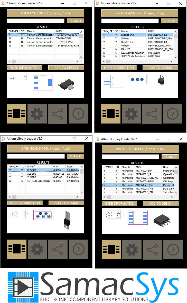
To design the schematic and PCB, I used Altium Designer 21, also the SamacSys component libraries (Altium plugin) to install the missing schematic symbols/PCB footprints. To get high-quality fabricated PCB boards, I sent the Gerbers to PCBWay.

To test the circuit, I used the power analysis feature of the Siglent SDS2102X Plus oscilloscope (or SDS1104X-E), Siglent SDL1020X-E DC Load, and Siglent SDM3045X multimeter. Isn’t cool, so let’s get started!

1142073422104t.jpg


1142583925320t.jpg


1144416457031t.jpg


References

Source: https://bit.ly/2VAxkV5

Altium Designer: https://www.altium.com/yt/myvanitar

SamacSys Altium plugin: https://www.samacsys.com/altium-designer-library-instructions

XL4016 schematic symbol, PCB footprint, 3D model: https://componentsearchengine.com/part-view/XL4016/XLSEMI

MCP6002 schematic symbol, PCB footprint, 3D model: https://componentsearchengine.com/search?term=mcp6002

TS4264 schematic symbol, PCB footprint, 3D model: https://componentsearchengine.com/part-view/TS4264CW50 RPG/Taiwan Semiconductor

MBR20100 schematic symbols, PCb footprint, 3D model: https://componentsearchengine.com/part-view/MBR20100CT-G1/Diodes Inc.

Siglent SDS2102X Plus oscilloscope: https://siglentna.com/digital-oscilloscopes/sds2000xp/

Siglent SDS1104X-E oscilloscope: https://siglentna.com/digital-oscilloscopes/sds1000x-e-series-super-phosphor-oscilloscopes/

Siglent SDL2010X-E DC Load: https://siglentna.com/dc-electronic-load/sdl1000x/
 

DC to DC buck converters is a famous topology in the electronic and a widely used circuit in electronic devices. A buck converter steps down the input voltage while it increases the output current. In this article/video, I have discussed a DC to DC buck converter that can be used effectively as a switching power supply. The output voltage and current are adjustable: 1.25V to 30V and 10mA to 6A (continuous). The power supply supports the constant voltage (CV) and constant current (CC) features. Two LEDs demonstrate the CV and CC status. The circuit is compact and both sides of the PCB have been used to mount the components.

To design the schematic and PCB, I used Altium Designer 21, also the SamacSys component libraries (Altium plugin) to install the missing schematic symbols/PCB footprints. To get high-quality fabricated PCB boards, I sent the Gerbers to PCBWay.

To test the circuit, I used the power analysis feature of the Siglent SDS2102X Plus oscilloscope (or SDS1104X-E), Siglent SDL1020X-E DC Load, and Siglent SDM3045X multimeter. Isn’t cool, so let’s get started!


1142073422104t.jpg


1142583925320t.jpg


1144416457031t.jpg


References

Source: https://bit.ly/2VAxkV5

Altium Designer: https://www.altium.com/yt/myvanitar

SamacSys Altium plugin: https://www.samacsys.com/altium-designer-library-instructions

XL4016 schematic symbol, PCB footprint, 3D model: https://componentsearchengine.com/part-view/XL4016/XLSEMI

MCP6002 schematic symbol, PCB footprint, 3D model: https://componentsearchengine.com/search?term=mcp6002

TS4264 schematic symbol, PCB footprint, 3D model: https://componentsearchengine.com/part-view/TS4264CW50 RPG/Taiwan Semiconductor

MBR20100 schematic symbols, PCb footprint, 3D model: https://componentsearchengine.com/part-view/MBR20100CT-G1/Diodes Inc.

Siglent SDS2102X Plus oscilloscope: https://siglentna.com/digital-oscilloscopes/sds2000xp/

Siglent SDS1104X-E oscilloscope: https://siglentna.com/digital-oscilloscopes/sds1000x-e-series-super-phosphor-oscilloscopes/

Siglent SDL2010X-E DC Load: https://siglentna.com/dc-electronic-load/sdl1000x/
Did you have specs for step load response vs results? or phase margin vs load?
 

I made some tests, the ringing was low and response was fast enough, however large output capacitors and a low side shunt might affect the response shape. The usefulness of these tests depends on the application.
 

The useful noise and ripple tests generally from my 20 yrs of Test Engineering experience were done is AC coupled to coax then 50 termination to scope rather than
1632322502376.png


This eliminates the crosstalk and probe gnd inductive pickup. Then you must increase step loads to find the stability margin instead of a steady load of max current. Then you will see how much overvoltage it has from stepping down to the minimum from all the stored energy in the reactive parts when demand drops to zero. This is the worst case and often a pre-load was necessary or active compensation.

With a 5 A swing choose a low side current shunt of 50mV or 10 mohms with a suitable amplifier that senses below 0V.
 
Thank you very much.
Even with a ground spring, it was picking inductive spikes that I had a doubt about the source.
There would not be any thermal stress on the 50-Ohm terminator?
 

Thank you very much.
Even with a ground spring, it was picking inductive spikes that I had a doubt about the source.
There would not be any thermal stress on the 50-Ohm terminator?
The ground spring might not be using the same gnd as the IC reference gnd.

Thermal stress? No because if it is only AC spikes. The 50R must also be short , cut down like a 1/4W part inserted in a BNC T at scope input , or better, SMD internal in DSO .

The plastic SMD or small ceramic RF C coupler must also be short in length from low ESR DC out cap to coax. ( few mm ).

Treat all power as you would logic ground and all control signals as Analog gnd ( i.e. isolated except IC control chip is connected to output low ESR caps for Vfb and 0V . If shared on a gnd plane to input , analyze the shared power paths for input and Vfb differential input .

If a design were DC isolated and there is a lot of feed-thru CM noise pulses then bridge them with an RF plastic cap. from Vout - to input Vin- to Earth gnd then fix the differential noise with array values with known C*ESR=T

After that , remove cap and add compensation pF caps to transformer to reduce the Vcm noise pulses which often get picked up by a probe.

YOu can never remove all ripple, otherwise voltage feedback would never detect ripple error. You would need current feedback as the primary control and 2ndary filters.
 

Status
Not open for further replies.

Similar threads

Part and Inventory Search

Welcome to EDABoard.com

Sponsor

Back
Top