Continue to Site

Welcome to EDAboard.com

Welcome to our site! EDAboard.com is an international Electronics Discussion Forum focused on EDA software, circuits, schematics, books, theory, papers, asic, pld, 8051, DSP, Network, RF, Analog Design, PCB, Service Manuals... and a whole lot more! To participate you need to register. Registration is free. Click here to register now.

low power high efficiency switching regulator (5V to -28V)

Status
Not open for further replies.

cocopa

Junior Member level 2
Joined
Feb 13, 2012
Messages
24
Helped
0
Reputation
0
Reaction score
0
Trophy points
1,281
Visit site
Activity points
1,508
Hello, I have a 5V power supply from which I want to produce -28V, @500uA max load current.
I've tried using lt1617-1 from linear technology but the simulation at LTspice shows an RMS current consumption of about 7-8mA, which is not acceptable for my application.
Any ideas on improving the circuit attached to lower overall current consumption (ideally around 1-2mA) or suggestions of any other implementations would be really helpful.
Thank you.
Pwer_supply_-28V.PNG
 

Hi,

but the simulation at LTspice shows an RMS current consumption of about 7-8mA,

RMS current isn´t valid for a swtiching regulator´s (input or output) power consumption --> use average current.

(RMS only makes sense for the inductor to calculate it´s power loss.)

Klaus
 
  • Like
Reactions: cocopa

    cocopa

    Points: 2
    Helpful Answer Positive Rating
you could use a 555 CMOS timer and external fet to run this ckt at 100kHz say, this would give you the lowest losses in the driving / control ckt... the chokes are often a source of loss in these ckts - for lowest losses you need to specify an RM6 say of N87 or better material run at low peak flux 150mT max say...
 

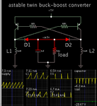
Here is a buck-boost converter, twin interleaved, astable operation. It draws average 3.7 mA from the 5v supply. It ignores losses due to parasitic resistances. The load is calculated as 56k ohms. Output is -28v to the load.

twin astable buck-boost 5v to -28v 500uA.png
 
  • Like
Reactions: cocopa

    cocopa

    Points: 2
    Helpful Answer Positive Rating
Do you need -regulation- or just a roughly right
negative voltage?

My last design at my first employer was a DC-DC
chip for "ringing SLIC" applications (negative boost
converter). Meant to produce -48V but could be
set arbitrarily. You might find similar and better
(been over 15 years since then) options in the TI,
Intersil/Renesas power management product lines'
telecom offerings. If you wanted regulation.
 

Here is a simple design based on an off-the-shelf gate drive transformer that gives should give good efficiency (~75 %). You will have some control over the output voltage using pot P1. The efficiency can be increased (~78 %) by omitting the snubbers, but you will have more EMC issues. The DC average value shown is with both snubbers in the circuit.
 

Attachments

  • 5_28_fb.png
    5_28_fb.png
    64.9 KB · Views: 242

Module selling for $10 (1Kpcs)
https://www.eetimes.com/document.asp?doc_id=1287903

Gonna be tough to beat that with a discrete parts-pile
and PCB of your own cobbling.

https://www.mouser.com/Maxim-Integr...-PMIC/MAX1856-Series/_/N-1yz3sqoZwnwwZ1yxz1ec

Roughly appropriate piece-part (uses a fancy looking
xfmr) at $4.60 (qty=1)

Maxim inverting dc-dc selector guide - w/ budgetary pricing even
https://para.maximintegrated.com/en/results.mvp?fam=invreg&tree=master

I'm sure you can find others of similar description
(Mr. Googlez was happy to cough up many hits for
"slic dc-dc").
 

The IC solution is obviously the best by far. The transformer in the design I posted cost $3 for one piece ($1.80/100pcs) from Digikey, and the rest should cost maybe $1-2 more, which can be a low-cost roll-your-own option. The OP never supplied more information regarding regulation requirement, which may make my proposal unacceptable anyway
 

A sepic, per post #1 at 70-100kHz driving a mosfet from simple CMOS 555 control, will give low cost and very high efficiency for low loss chokes, and 45V schottky diode.
 
Last edited:

E-design, RC snubber directly across T1 might release the need for D2. What do you think?

It should not make a significant difference. Below are both results (with D2 out), and it is hard to spot any difference.

In general, we can do away with D2 when using the gate transformer with guaranteed known maximum leakage inductance, but otherwise with sloppy construction you can cause a reverse breakdown in T1. I don't think it hurts to keep D2 as it consumes less than 40 uW of power in this instance.
 

Attachments

  • snub_pos.png
    snub_pos.png
    19.6 KB · Views: 243
  • Like
Reactions: CataM

    CataM

    Points: 2
    Helpful Answer Positive Rating
Many of the chips available have high efficiency at rated full load, but not at very light loads.
 

Attachments

  • Eff.png
    Eff.png
    34.2 KB · Views: 226
  • Eff_1.png
    Eff_1.png
    24.1 KB · Views: 217

CataM: the sepic with o/p diode and L swapped over, per the fig in post #1 sometimes called a Zeta converter, does produce a neg output.

Sepic, stands for Single ended primary inductance converter, and can be used to describe all such topologies, Sepic, Zeta, Cuk, etc
 
  • Like
Reactions: CataM

    CataM

    Points: 2
    Helpful Answer Positive Rating
If regulation is required we can use the spare gate to implement some burst-mode regulation. This will push the efficiency near/over 85%.
 

Attachments

  • 5_28_fb_reg.png
    5_28_fb_reg.png
    59 KB · Views: 232
  • 5_28_fb_reg_1.png
    5_28_fb_reg_1.png
    19.3 KB · Views: 217

Status
Not open for further replies.

Similar threads

Part and Inventory Search

Welcome to EDABoard.com

Sponsor

Back
Top