Continue to Site

Welcome to EDAboard.com

Welcome to our site! EDAboard.com is an international Electronics Discussion Forum focused on EDA software, circuits, schematics, books, theory, papers, asic, pld, 8051, DSP, Network, RF, Analog Design, PCB, Service Manuals... and a whole lot more! To participate you need to register. Registration is free. Click here to register now.

Boost Converter Gate Voltage distortion and Gate Resistor effect on load current

Status
Not open for further replies.

basit701

Newbie level 6
Newbie level 6
Joined
Sep 22, 2017
Messages
12
Helped
0
Reputation
0
Reaction score
0
Trophy points
1
Visit site
Activity points
130
Hello Guys! Hope you are doing great.

I am making a Boost Converter from 40V DC to 370V DC. I previously patched the circuit on breadboard but due to stray inductance and capacitance, i moved to deadbug prototyping (distortion is negligble now). The components i am using are:

Inductor: 1.5mH
Diode: MUR860 8A 600V ultra fast
Capacitor: 220uF 450 Volts
MOSFET: 47N60C3, 35N60C3, IRF 450 and some IGBTS lying around.
Load: 2 x Candescent Bulb (Total Resistance of two bulbs = 88ohms).
Gate Driver: TLP250 (Gate resistor connected in series with a pull down resistor of 2k ohms connected across Gate and Source)

So far i have successfully boosted the voltage (not to the desired one) from 40V but i am experiencing some weird problems.
1) The gate voltage when mosfet is switching has some distortion during turn on and off. (You can see in the oscilloscope result in the picture attached).

2) Changing Gate Resistor changes the Drain current of the mosfet. E.g. on 47N60C3 at 17ohms gate resistance the mosfet current is maximum (saturates at 3A due to supply limitation) and the bulb glows brightly however the gate voltage is not purely square due to RC circuit with comparatively large R so time constant is more. If i reduce the gate resistor e.g. 5ohms then the gate voltage becomes much more square wave one but the current capabablity off mosfet decreases (current reduces to 1.8A and bulb brightness decreases). Both of these test have been performed on constant input voltage and constant frequency with constant duty cycle. I HAVE OBSERVED THIS THING ON OTHER MOSFET AND IGBTS also. I also performed some test i.e. i connected Rg = 60 ohms and got Vout =260V at 72% duty cycle, then i reduced Rg = 40 ohms but got Vout = 260 after changing duty cycle to 77% (PIcture Attached)
 

Attachments

  • 21931638_2182546218437438_816577640_o.jpg
    21931638_2182546218437438_816577640_o.jpg
    130.7 KB · Views: 126
  • 21951418_2182545885104138_1441437295_o.jpg
    21951418_2182545885104138_1441437295_o.jpg
    138.6 KB · Views: 137

Hi,

Instead of writing long text --> post your exact schematic.Here the picture give additional informations of all connections.
But don't post a photo with just a couple of numbers and characters.Here the picture gives no additional informations.


Klaus
 

As in the prototype developed picture attached,
for point no.1 There are few hanging wires, and if your G-E are hanging gate voltage will be of distortion,whenever the igbt is switched.You can twist gate emitter wire and keep it at shortest distance.If possible design a small board with MOSFET and GD on the same board without any looping and shortest distance.
for point no.2 I dont understand how gate resistance changes your device current limit, if it was gate voltage amplitude change i would have accepted.
Please post the waveform.

Thanks,
Mukesh
 

Everything can happen in the shown "wire entanglement" with huge parasitic inductance. If you connect a probe tip somewhere and the ground clip at another node assumed to act as "ground", it's hard to tell if the acquired waveform is actually the Vgs voltage of interest.

Similarly it's not obvious at first sight which effects changing the gate resistor brings. Switching the transistor faster can under circumstances cause Vds overvoltage driving the FET into avalanche breakdown. Or increase diode recovery losses.

I'm not sure if it's possible to figure out the effects in this circuit layout. To try at least, you'll look at clear oscilloscope waveforms acquiring Vgs and Vds simultaneously. Doesn't your oscilloscope provide a hardcopy to USB stick or similar?

How to measure Vgs then if acquired waveform is not actual Vgs?

Also I could'nt get the the avalanche breakdown you talked about. How Vds overvoltage can occur? my input voltage is not greater than 40 V and how faster switching can lead to avalanche breakdown?

Yes the oscilloscope do have USB port. I was in hurry yesterday o could'nt copy the results in USB.
 

How to measure Vgs then if acquired waveform is not actual Vgs?
By probing directly at the transistor, preferably with a short ground cable or bayonet ground tip.

- - - Updated - - -

How Vds overvoltage can occur? my input voltage is not greater than 40 V.
I'm only considering possible effects in lack of significant measurements. 40 V doesn't count, the intended boost output voltage of 370V isn't so far from IR450 Vds rating. And there may be overvoltage at MOSFET drain by the working of parasitic circuit inductance.

But I'll stop guessing here, the actual waveforms want to be measured.
 

here is pcb layout guide for smps.............all circuits with high di/dt, and indeed all other circuits, shoudl have minimum area enclosed in their loop.
Also, avoid power switching currents going through lengths of control gnd.
 

Attachments

  • Basics of SMPS Layout _4.doc
    645.5 KB · Views: 149
here is pcb layout guide for smps

An excellent document for every student of power (supply design)!
 
  • Like
Reactions: treez

    T

    Points: 2
    Helpful Answer Positive Rating
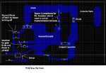
I have made this PCB (15x8 cm). Is this correct? I tried to minimise loop area.PCBsample.png
 

Hi,

Some keys to success:
* a schematic
* GND plane
* short traces
* fast capacitors

Klaus
 

well in #9 i dont see your sense resistor which i presume is in the source?.....you tend to make the gnd temrinal of the source sense resistor the "star ground" point.
But the stipulations are not new ones, its the same old thing as i stated before in post above

all circuits with high di/dt, and indeed all other circuits, shoudl have minimum area enclosed in their loop.
Also, avoid power switching currents going through lengths of control gnd becausr this can cause ground bounce.

,...Basically, dont make loop antennas and dont cause ground bounce.....that can be your mantra.....the high di/dt in the stray inductance of the tracks can cause ground bounce.
 

....the high di/dt in the stray inductance of the tracks can cause ground bounce.

Sound advice every student should learn. Sometimes it may be even prudent to reduce the di/dt, at the cost of higher dissipation, just to increased assurance of greater stability. Stability is a greater virtue.
 

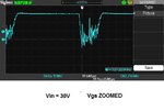
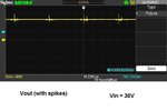
Okay guys so i made the PCB and was hoping that distortion willl end but to my surprise the distortion is still there. Distortion at gate was more when Vin was 30 compared to Vin =10 V. I am attaching the scope results for reference. I have used snubber at gate (Grounding resistor and UF4007 anti parallel)Capture.JPGSDS00001.jpgSDS00002.jpgSDS00003.jpgSDS00004.jpgSDS00005.jpgSDS00007.jpgSDS00008.jpgSDS00009.jpg
 

Where is the 0.1 uF bypass cap between pin 5 and 8 of the gate driver?
I believe stray PCB inductance causes the ringing at higher Vin because of higher Vds which the FET needs to switch. A turn off resistor might attenuate the ringing at turn off.
 

Hi,

We (and the datasheet) recommend" short traces. This means a couple of millimeters and surely not a couple of centimeters.
And all the other recommendations we gave...it seems you didn't read.

The PCB layout is not suitable. Malfunction is expectable. Read post#10 ... and best: all others and the datasheets, too.

Klaus
 

I have realised that PCB layout is flawed. I am working on new layout according to post #10. I have one question in mind. Do the power leads (input to boost from power supply and output from iti to the load) needs to be short?. The minimum length i could achieve due to space constraints is 12cm. Should i use twisted pairs? Or shielded wire with shield connected fo ground?
 

Status
Not open for further replies.

Similar threads

Part and Inventory Search

Welcome to EDABoard.com

Sponsor

Back
Top