Continue to Site

Welcome to EDAboard.com

Welcome to our site! EDAboard.com is an international Electronics Discussion Forum focused on EDA software, circuits, schematics, books, theory, papers, asic, pld, 8051, DSP, Network, RF, Analog Design, PCB, Service Manuals... and a whole lot more! To participate you need to register. Registration is free. Click here to register now.

20A smps battery charger

Status
Not open for further replies.

freeman3020

Member level 1
Member level 1
Joined
May 20, 2014
Messages
37
Helped
1
Reputation
2
Reaction score
1
Trophy points
8
Visit site
Activity points
279
Hi all

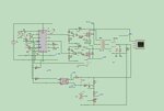
I designed 20A charger using tl494 ,the problem mosfet damaged many time one I connect mains rectified DC volt, also IC damaged,
I tried circuit without feedback many time so duty cycle 45% without any problem, I think when duty cycle close to 0 , mosfet bomb ,I think I need some component for protection

tl494-4.jpg
 

The "interlock" diodes D6/D7 look suspicious, not a serious circuit design means.

I don't see what's the specific problem with "duty cycle close to 0", provided the transistors are switching regularly.

There should be RCD snubbers absorbing the drain overvoltage spikes due to transformer leakage, the dimensioning must be checked empirically with loaded output.

By design, the converter has no means to detect flux walking or transistor overcurrent.

D6/D7 are 12 volt zener diode for protection

can you explain how to add RCD snubbers absorbing? I searched and found it used in flyback not push pull topology
 

you already put zener d4 and d5 for gate protection d6 and d7 no need also your d7 is grounding the gate drive pulse
 

Sorry d4 and d5 are zeners
d6/d7 are diodes

the wrong on drawing .

I correct it

tl494-4.jpg

is there need to remove d6/d7
 

No need d6 and d7 Its better to put ferrite core isolating transformer for driving the power mosfet what is your main rectified voltage
 

with a push pull, all you need is mosfet driver to drive mosfets.
But i done know why you put the pnp turn off circuit in there...that is only needed for hi side drives...pushpull doesnt have hi side drives.

Pushpull is a not that good, there is always not perfect coupling between the primary halves of coils, and you need to quench the leakage spikes.
 

The circuit has some errors.How Q2 works ??All terminals seems connected to GND while Emitter of Q1 is connected to source(?) ??
 

D6/D7 should be removed. They will push the drivers towards self-oscillation, which you don't want.

Q1 and Q2 are in a fairly standard configuration. Though D4/D5 should not be necessary.

The other major flow is the lack of an energy storage inductor on the secondary side. Without that, it can't even be called a push pull converter. You'll have limited ability to control the average output current/voltage, and you'll get tremendous ripple currents.
 

Status
Not open for further replies.

Similar threads

Part and Inventory Search

Welcome to EDABoard.com

Sponsor

Back
Top