Continue to Site

Welcome to EDAboard.com

Welcome to our site! EDAboard.com is an international Electronics Discussion Forum focused on EDA software, circuits, schematics, books, theory, papers, asic, pld, 8051, DSP, Network, RF, Analog Design, PCB, Service Manuals... and a whole lot more! To participate you need to register. Registration is free. Click here to register now.

lt3750 capacitor charger problem

Status
Not open for further replies.

gorkemsay

Newbie level 4
Newbie level 4
Joined
Sep 12, 2017
Messages
6
Helped
0
Reputation
0
Reaction score
0
Trophy points
1
Visit site
Activity points
68
Hey guys im new here and this is my first message in this forum. i want to talk about some problems about the LT3750 capacitor charger.

Im trying to design a 240V 6A capacitor charger system. i have made calculations according to lt3750 datasheet. then i have construct the circuit in breadboard (yeah i did this). the circuit has worked but not reliable and desired voltage. it has charged to about 100V around.... i think that can be arise from breadboard and i havent use exactly same values. then i decided to design pcb i have designed and constructed the pcb. i have used exactly same value of components. but i didnt work. i have checked thousand times pcb there is no mistake about routing ways placements..... i have connected the Vtrans and Vcc to each other to 12V. i have connected the CHARGE pin to arduino digital output high. i have checked the gate pin with oscilloscope there isnt any reaction. is there any idea about it?

- - - Updated - - -

if there is someone to share their idea or can help, i can give more details.
 

Hi,

This is no circuit for a breadboard.
Or vice versa: A breadboard is not suitable to thest such "switching power" circuits.

--> Use a PCB according the board layout recommendations of the datasheet.

Klaus
 

Yeah thats right. In my country its not simple to make thats kind of pcb. thats why i construct in breadboard first. anyway i have made the pcb too.
 

I've successfully built a capacitor charger using a LT3750. It works well, but board layout and bypass capacitors matter a lot. My first PC board didn't work at all; the LT3750 wouldn't switch. It took a while to find a layout that would work.

(Unable to upload image due to bad forum configuration. Error message: "Od dnia 1 sierpnia 2017 roku uploader obrazków Elektroda jest dostępny tylko dla zalogowanych użytkowników forum Elektroda. Dzięki temu w przyszłości udostępnimy możliwość zarządzania zdjęciami. Za chwilę zostaniesz przekierowany pod nowy adres uploadera obrazków, jeśli to nie nastąpi kliknij tutaj.

Starting from 1 August 2017 the Elektroda Image Uploader is only available for logged Elektroda users. Thanks for this we will be able to offer you manage your images. Please click here if you are not redirected within a few seconds."
I am already logged into the EDA board. I'm not going to sign up for some strange upload service.

Look, moderators, if you're going to demand that users use your upload service for all images, fix the upload problem. I was going to post a detailed explanation, with board layouts, of how to deal with LT3750 problems. Because of this failure by the forum operators, I won't. Can anyone suggest a better-run EDA forum?)
 

(Unable to upload image due to bad forum configuration.
...
I am already logged into the EDA board. I'm not going to sign up for some strange upload service.

Look, moderators, if you're going to demand that users use your upload service for all images, fix the upload problem.

I get success by uploading images to 'My Attachments'. I do not use the Electroda site.

Edaboard provides a personal area for each member to store images and files. Steps to access it:

(1) Click 'Go Advanced' (opens a Reply window with several options).
(2) Click 'Manage my attachments'
(3) Upload image from your computer using the navigation windows.
(4) Add image to your post by dragging it into lower window.
 

I agree that the non-functional button "Add an image" is confusing. You can use the small "Insert Image" tree icon instead.
 

(OK, so "Upload image" and "Manage Attachments" are completely different systems. Whatever.)

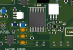
lt3750board3d.png
Successful LT3750 layout.

U1 is the LT3750. The big MOSFET above is its switch. The transformer is to the left.
All the passive components it needs are tightly clustered around it. The traces in that area have as few crosses and vias as possible.

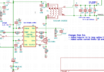
lt3750schematic.png
The schematic of that section

Note all those bypass caps: C8, C9, C11. The data sheet says you need those, and you do. C12 and L1 are to keep current spikes from the switcher from getting back into the upstream power circuitry and causing trouble. U2, the inrush current limiter for USB ports, sees any back-current as a fault condition and shuts down. There's a 20ns back-current spike when Q1 switches off and T1 dumps.

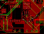
lt3750charger1.png
Board layout

There's a keep-out area along the inside of the pads for U1 to prevent traces from going into the pads from the "wrong" side. This causes soldering problems. The keep-out area is narrow, so that GND fill goes down the middle.

By the way, this was all auto-routed by FreeRoute in KiCAD. Component positions were adjusted until the routing came out well.

- - - Updated - - -

**broken link removed**
Detail of the critical layout area

Here's a close-up of the critical area of the layout. This follows the suggested layout in the data sheet, but with real part sizes.

This stuff matters. This circuit generates huge spikes with very fast rise times. The LT3750 works by turning flip-flops on and off with fast comparators, and if some unwanted spike trips a comparator early, it won't work. Those bypass caps have to be near the trouble spots, as the data sheet says, and they have to be low-ESR caps to absorb the spikes.

Incidentally, the original poster mentioned driving the CHARGE pin from an Arduino. That's fine, but be aware that it's the edge (OFF to ON) that triggers the CHARGE pin. If the CHARGE pin is high when power turns on, nothing will happen until the next OFF-ON transition.

A few other notes:

- It's helpful to simulate this in SPICE. Get rid of all the unwanted spikes and glitches in the SPICE model. (There may still be real-world spikes due to layout problems, but any trouble seen in the SPICE model will usually be there in the real world.) It's worth looking at what the LT3750 is doing in SPICE. Watch the current in the transformer primary and the voltage at the current sense resistor, and see the gate turn off when the threshold is crossed. On the real hardware, watch the same thing happen on a scope. They're reasonably close when you get it working right.

- Those strange parts M1, M2, etc.? Those are dummy "narrowers" to connect a wide trace to a narrower trace. KiCAD doesn't do "necking" well, and without that, you can't connect a wide trace to the tiny 0.5mm pitch pins of the LT3750.

- In layout, it's helpful to have a footprint for the LT3750 which has no bare copper under the raised part of the pins. If you have copper there and you get a solder bridge under the raised part of the pins, getting it out is really tough. (I had a very difficult hour doing rework under the microscope with the first board design.)

- Note that the output diode D1 has to have really fast recovery. The data sheet points this out. The data sheet recommendations on MOSFET, transformer, and output diode are important.

Once you get all this right, it's a great cap charger. Its strategy for running the switcher is near-optimal.
 
Hi,

It took a while to find a layout that would work.
The datasheet includes a section called "board layout considerations".
It includes a textual description as well as a board layout example.

They additionally have "design notes" and a "demo board" and so on.
Just go through this site: https://www.linear.com/product/LT3750#overview
Mind the menue on the left side.
This should prevent you from spending too much time to make it running.

Klaus
 
First of all, thanks for these very helpful information and for sharing your experience. i ll design a new pcb and i ll consider your recommendations.

-The other reason can be arise from through hole components. Also i ll order low-ESR capacitors this time.
-For arduino, digital pin goes HIGH in 2 seconds after powers ON but it never goes OFF.
-for ltspice, to be honest i have never used this spice before. but i ll do my best to do it. In the website of linear, there is a ltspice demo. it ll be helpful too.

but i got the main reasons. the pcb layout and components.
i was thinking the cause of not working is something else. Because there isnt any reaction. i was expecting to work but maybe not properly. but worked.

when i try the improvements, i ll post the results. thanks for help to everybody.
 

Hi,

i was thinking the cause of not working is something else. Because there isnt any reaction. i was expecting to work but maybe not properly. but worked.

So, if you trust in the datasheet, but you see that your circuit is not working... then there should be a difference between your circuit and the datsheet circuit.
If you want us to verify this, then you need to give use the chance by providing your circuit informations.

Send us your complete schematic, howy you built your circuit. Give us details (part numbers, names, specifiactions...) of the devices you used. Send us a picture of your complete breadboard circuit. Measure and give us all the voltages / scope pictures of the LT3750 in your circuit.

Klaus
 

here are my works. i have change somethings on pcb so it has worn a little bit.

- diode is rhrp30120
- mosfet is FR3710Z
- charged capcitor is 680uF 400V
- 150uF capacitor is electrolytic capacitor.

pcb has been manufactured by me by using photoresist pcb. after that all ways have been soldered.
 

Attachments

  • cap chg sch.png
    cap chg sch.png
    37 KB · Views: 187
  • cap chg brd.png
    cap chg brd.png
    65.6 KB · Views: 179
  • 20170913_125152.jpg
    20170913_125152.jpg
    434 KB · Views: 186
  • 20170913_125056.jpg
    20170913_125056.jpg
    442.4 KB · Views: 198

Hi,

This is as far away from PCB recommendations as can be. Maybe it works, but if, then not that clean as it should.

Your GND builds a nice loop antenna. No chance to comply with EMI regulations.


Klaus
 
Update!

Okay, after few days, i have design the pcb layout again. Finally it works. i have obtain desired voltage. But there is one more problem. when it charges the capacitor to desired 235 V, it stops charging. The capacitor starts decharging slowly. But it never starts new charge cycle. The datasheet says "When voltage of RBG equals 1.24V, charging is disabled."

When the charge starts, the rbg pin voltage starts to increase. when the rbg voltage exceeds the 1.24V, it stops the charging cycle. but when rbg voltage starts to decrease from 1.24V to 0V, it never starts a new charge cycle. i have measured the rbg pin voltage it shows 5mV around. shouldn't start a new charge cycle? or should i start it with charge pin again?
 

Update!

Okay, after few days, i have design the pcb layout again. Finally it works. i have obtain desired voltage. But there is one more problem. when it charges the capacitor to desired 235 V, it stops charging. The capacitor starts discharging slowly. But it never starts new charge cycle. The datasheet says "When voltage of RBG equals 1.24V, charging is disabled."

When the charge starts, the rbg pin voltage starts to increase. when the rbg voltage exceeds the 1.24V, it stops the charging cycle. but when rbg voltage starts to decrease from 1.24V to 0V, it never starts a new charge cycle. i have measured the rbg pin voltage it shows 5mV around. shouldn't start a new charge cycle? or should i start it with charge pin again?

That's what's supposed to happen. You won't get another charge cycle until you turn CHARGE off and then ON again.

This part is for when you need to charge up a capacitor for something like a camera flash unit. If you want a continuous output, this is the wrong tool for the job.
 
Status
Not open for further replies.

Similar threads

Part and Inventory Search

Welcome to EDABoard.com

Sponsor

Back
Top