Continue to Site

Welcome to EDAboard.com

Welcome to our site! EDAboard.com is an international Electronics Discussion Forum focused on EDA software, circuits, schematics, books, theory, papers, asic, pld, 8051, DSP, Network, RF, Analog Design, PCB, Service Manuals... and a whole lot more! To participate you need to register. Registration is free. Click here to register now.

Zero Load Switching Losses

Status
Not open for further replies.

asdf44

Advanced Member level 4
Joined
Feb 15, 2014
Messages
1,000
Helped
355
Reputation
710
Reaction score
344
Trophy points
1,363
Visit site
Activity points
9,716
Bringing up a new full bridge ZVS converter (400Vin) the first thing I did was run the primary bridge with zero load - the xfmr was de-populated thus both switched legs of the first full bridge went nowhere.

I expected to see low losses, verify that the circuit could handle full Vin and move on but I immediately saw losses steeply increase as I applied input voltage. Using 650V fets in 8x8mm SMT packages 'high losses' means something like 1-3W here.

First I assumed it was shoot-through but I quickly ruled that out (digital control meant I could easily adjust dead-time).

Ok so help me understand the variables here because it's not adding up. The only thing that 'should', as I currently understand it, cause switching losses in this scenario is output C - Coss (specifically Coss energy related - Cosser) plus whatever board parasitics there are. Is that right? Switching speed and gate drive should be irrelevant - the losses from charging and discharging Cosser X times a second are the same regardless of how fast it happens.


Fast forwarding three things helped me address this. First, the obvious - lower switching frequency (from 200 to 166). Second adding a load helps - ok fine is a ZVS topology when there is load so it makes some sense that losses could go down with load.

But finally, I ordered a variety of alternate fets from different manufacturers and saw different results and specifically got great results from Transphorm GAN fets (after addressing gate drive glitching from the high dv/dt and low Vgs threshold). But the results don't correlate with published Cosser or the energy storage versus volts chart of these devices. The GAN fet output C and stored output energy is higher than my first choice yet zero load switching losses are less - what am I missing?
 

In playing with eGaN FETs during a driver chip design
I found that source impedance on the high side FET
is a really big deal - the Qgg needs somewhere to go,
and fast, if you want efficient turnoff and letting it be
leisurely makes you spend time in dissipative conduction.

No load condition means high high-side source impedance.
Similar issues apply to MOSFETs I think, which is why
you see things like "near zero current switching" - you
want to switch when there's still some source current
running, so that current can "pull out" the gate charge.

Transphorm FETs, which last I looked are GaN FET over
LV Si MOSFET cascode structure, probably just act
different.
 
  • Like
Reactions: asdf44

    asdf44

    Points: 2
    Helpful Answer Positive Rating
Hi,

We don't see a schematic, so all we can do is guessing.

Switching speed and gate drive should be irrelevant - the losses from charging and discharging Cosser X times a second are the same regardless of how fast it happens.
I assume you are wrong here. All energy you need to switch ON a FET (gate charge including miller effect) has to be supplied.
But at switching OFF it is not stored back to thepower supply capacitor, instead it is dissipated to heat.

And often directely (via resistor) supplied by the 400V input voltage. This means every mA of gate drive current causes 1mA x 400V = 400mW of dissipated power.

Klaus
 
  • Like
Reactions: asdf44

    asdf44

    Points: 2
    Helpful Answer Positive Rating
I wonder what the term "ZVS" actually addresses in your post. An unloaded H-bridge is hard switching and involves respective switching losses, primarily caused by charging transistor output capacitances and to a lesser extent parasitic board capacitances.

If your circuit actually achieves zero voltage soft switching under normal load conditions, the switching losses can be reduced to a small fraction. Does it?

The "energy related" output capacitance doesn't cover the total switching losses in a hard switching push-pull circuit by the way. Due to the non-linear capacitance characteristic, most losses are caused by charging the off-state transistor.

ZVS is just part of the common name for this topology. So it seems you agree with my proposal that output C should dominate hard switched 'zero load' losses?

Yes, it appears that with increased load switching losses (in-fact total losses) decrease to acceptable levels before increasing again as resistive losses take over. But no-load is going to be a valid operating point for this converter so it must handle it (let me be careful - 'zero load' described the scenario when my transformer wasn't even populated. 'No-load' means the circuit is fully populated but no external load is applied. Both scenarios have been similarly problematic although with the transformer populated magnetizing inductance means there is a small amount of conducted current).

Well as it happens Cosser has typically been specified at my input voltage of 400V so it should be a proxy for energy stored at a Vds of 400? But anyway, I've largely been skipping that parameter and referring to the stored energy versus Vds charts that are supplied and that's what I'm going on when I say the GAN fets have higher energy storage than the silicon fets I'm comparing them too (yet lower zero load hard switched losses).

Yes I was reminded the hard way that Coss is exceedingly non-linear since I started seeing fairly substantial switching losses as low as 20Vin which made me assume something was catastrophically wrong - but losses stopped going up steeply beyond that point which matched the Coss curves in the data sheet.

Hi,

We don't see a schematic, so all we can do is guessing.


I assume you are wrong here. All energy you need to switch ON a FET (gate charge including miller effect) has to be supplied.
But at switching OFF it is not stored back to thepower supply capacitor, instead it is dissipated to heat.

And often directely (via resistor) supplied by the 400V input voltage. This means every mA of gate drive current causes 1mA x 400V = 400mW of dissipated power.

Klaus

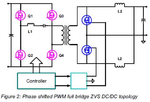
Klause for the purposes of this discussion any 'phase shift zvs' schematic should suffice:
**broken link removed**

I don't follow. I fully understand that driving the gate consumes energy but the component that's 'burnt up' within the fet should be small, and in-fact I see no visible heating when the gate drives are on prior to applying input voltage. The gate drive power is supplied by a separate isolated supply that hasn't entered the discussion yet.

Or are you saying that gate drive current induces drain
 

A "ZVS topology" must involve a means for soft switch commutation, like a LLC converter. I don't yet understand if your converter circuit does.

Cosser or Co(er) can be used to calculate the Coss related switching losses of a single ended switch, e.g. a hard switching boost converter.

Gate charge and -power can be ignored for the discussion, I presume.
 

Referencing the schematic I linked above this topology can ZVS when there is sufficient energy stored in L1 to commutate the loop and appropriate dead-time to allow that to happen. Realistically that means it ZVS's at medium to high load currents but won't fully ZVS at lighter loads and effectively hard switches at no-load (with only magnetizing current flowing through L1).

Ok so back to my question, in a no-load or zero-load hard switched scenario why might my GAN fets have lower losses than my silicon fets despite the fact that they have higher Co(er) at the specified input voltage?
 

Referencing the schematic I linked above this topology can ZVS when there is sufficient energy stored in L1 to commutate the loop and appropriate dead-time to allow that to happen.
The schematic seems to be sketched a bit sloppily, as it doesn't differentiate between transformer main and leakage inductance. With sufficient low main inductance (air gap required), the circuit can well work as ZVS + ZCS converter.

Main inductance will be usually ten times larger than transformer inductance + L1, in so far main inductance rather than L1 is the dominant commutation means.

- - - Updated - - -

GAN fets have lower losses than my silicon fets despite the fact that they have higher Co(er) at the specified input voltage?
As already stated, Co(er) is underestimating hard switching losses in push-pull operation. If I remember right, the on+off loss total is relative to 2*Co(tr) (Co(tr) = "time related" or average output capacitance).
 
  • Like
Reactions: asdf44

    asdf44

    Points: 2
    Helpful Answer Positive Rating
The schematic seems to be sketched a bit sloppily, as it doesn't differentiate between transformer main and leakage inductance. With sufficient low main inductance (air gap required), the circuit can well work as ZVS + ZCS converter.

Main inductance will be usually ten times larger than transformer inductance + L1, in so far main inductance rather than L1 is the dominant commutation means.

- - - Updated - - -


As already stated, Co(er) is underestimating hard switching losses in push-pull operation. If I remember right, the on+off loss total is relative to 2*Co(tr) (Co(tr) = "time related" or average output capacitance).

By 'main inductance' I assume you mean magnetizing inductance. I believe it's not common to rely on magnetizing current to commutate the loop in this topology because any magnetizing inductance that supplies enough current to commutate at light loads amounts to a wasteful amount of extra circulating current at every other operating point. Also the control scheme means that when its commanded to put out near zero output voltage there will be no magnetizing current either yet the primary fets still switch continuously at full speed 50% duty cycle.


I don't understand how Co(tr) factors in at all. Co(er) tells you the energy stored and its energy that needs to be charged/discharged/dissipated every switching cycle...

...Though my mind is forming an idea where perhaps I can see how resistively charging a non-linear capacitor might result in an asymetry between the amount of energy stored in the capacitor versus the energy dissipated in the resistor during the charge...is that what you're getting at?
 

I believe it's not common to rely on magnetizing current to commutate the loop in this topology because any magnetizing inductance that supplies enough current to commutate at light loads amounts to a wasteful amount of extra circulating current at every other operating point.
Read a bit about LLC converters to see that it's a commonly used method.

Wasteful amount is a good point. Generating an additional current makes sense if reduces overall losses.

I was referring to Co(tr) because it's specified in some datasheets, e.g. from Infineon. The relation of Co(er) and Co(tr) is a measure of output capacitance non-linearity. The smaller the energy related capacitance compared to average "time related" value, the larger the ratio of switch-on energy loss to Coss stored energy.

Charging and discharging the non-linear capacitance through a resistor is a simple way to visualize the asymmetrical losses in push-pull operation.
 

The Coss related switching losses of a half bridge can be calculated as follows.

Bus voltage = Vdc,
voltage dependent output capacitance = Coss(Vds).
Transistor Q1 is turned on, initial Vds1 = Vdc, final Vds1 = 0. Transistor Q2 is charged at the same time, initial Vds2 = 0, final Vds2 = Vdc.

Code:
Esw,tot = Esw1 + Esw2 
        = ∫Coss(V) V dV +  ∫Coss(V)(Vdc - V) dV 
        = ∫Coss(V) Vdc dV
        = avg(Coss(V) Vdc²

or referring to the datasheet quantities Co(er) and Co(tr)
Code:
Esw,tot = Esw1 + Esw2 
        = 0.5 Co(er) Vdc² +
          (Co(tr) - 0.5 Co(er)) Vdc²
        = Co(tr) Vdc²
 
  • Like
Reactions: asdf44

    asdf44

    Points: 2
    Helpful Answer Positive Rating
Hi,

Klause for the purposes of this discussion any 'phase shift zvs' schematic should suffice:
ZVS1.png

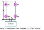
If I understood correctely ... you said the transformer is not connected.
Then this circuit is remaining:
ZVS2.png
Where exactly in this circuit do you measure the current?
What exactley is the capacitor type?
Do you see any oscillation?
Can you hear any sound? Maybe there is ultrasound caused by any piezoelectric effect?

I fully understand that driving the gate consumes energy but the component that's 'burnt up' within the fet should be small,
I agree. Most of this energy is dissipated by the driving circuit, and not inside the MOSFET.

Klaus
 

Where exactly in this circuit do you measure the current?
What exactly is the capacitor type?
I presume, switching losses of the unloaded H-bridge are determined my measuring the average DC input current. As long as Vdc ripple is low, the capacitor type doesn't matter much in this test setup.
 

Hi,

I agree.

I try to call everything into question:
These are just ideas, and maybe the OP can all these issues exclude within seconds.

* Can we be sure that the voltage ripple is low?
What if the capacitor is a ceramics capacitor.. and there is some kind of resonance causing voltage ringing.. in this causing mechanical power dissipation.

* Maybe it is a non suitable electrolytics capacitor.. combined with some ripple voltage/current?

* Is he really measuring averaged DC current? Maybe he is measuring RMS current including the ripple current, so he sees a (parto of) current that doesn´t cause power dissipation.
(An idea because he calculates 1..3W, but this should cause temperature rise. Recognizeable with the touch of a finger)

Klaus

7x10uF electrolytics plus 7 470n ceramics (and power and ground planes that are deliberately interleaved across the 8 layers for additional plane-plane C). I have looked at input current with a high bandwidth current clamp and ripple is reasonable (probably <15%)

I've actually been focusing on temperature using a high res IR camera rather than losses specifically since temperature is what matters at the moment. When I'm talking about 'high losses' I'm talking about fets that are burning up - shooting towards 100C before I slam the power button or sitting at 95C with only 200Vin (these tiny packages don't have much thermal margin for error). So I haven't always been recording watts rigorously in instances when the device is clearly not going to cut it though I do believe that input current (losses) and temperature are correlating well.

The GAN fets stayed between 60 and 80C across my entire application V/I output area for example and let me evaluate the rest of the design. Thankfully everything else is if anything better than I anticipated and I'm seeing peak efficiencies in the low 90's.

Anyways for what its worth when I post threads like this I try to generalize somewhat rather than simply asking people to fix my specific circuit and in this case I wanted the discussion to center on these hard switching losses which I realized I didn't understand as well as needed.


When I have more time I'll analyze the other responses more closely. Thanks.
 

Most of this energy is dissipated by the driving circuit, and not inside the MOSFET.

Careful. This is an expression of the goal, an ideally "tuned"
powertrain. It is not necessarily the case in hand. If the
gate drive is not ideal then there will be time spent in
conduction that is not ideally "on" or "off" and then comes
the heat.

A look at sensitivity to high side / low side phasing in the
dissipation and the source current / drain current wvfms
in HSS and LSS is worth something. It's quite possible that
gate drive needs to move, based on load-point, to get
light load efficiency. Have seen this done closed-loop for
high side switch control in (near) zero current switching
topology.

In these power totem-poles you want a "clean handoff"
from LSS to HSS and vice versa. Deviating in either direction
raises dissipation (cross conduction, or excess "open time",
especially once you get the inductor in the mix to enable
flyback voltage to be imposed on weakly commutating
FETs).
 

Hi,

@dick_freebird:
I was talking about gate_drive_energy only.

Klaus
 

When I'm talking about 'high losses' I'm talking about fets that are burning up - shooting towards 100C before I slam the power button or sitting at 95C with only 200Vin (these tiny packages don't have much thermal margin for error). So I haven't always been recording watts rigorously in instances when the device is clearly not going to cut it though I do believe that input current (losses) and temperature are correlating well.

Sounds reasonable so far. Once you have verified that the majority of losses is located in the MOSFETs, it makes sense to measure the input current to check if the losses fit the expectable level calculated in post #11 or if you experience excessive losses due to shoot through, either caused by insufficient dead time or parasitic transistor turn on. Reducing the positive gate current (slowing down turn-on) for test can clarify this.
 

    V

    Points: 2
    Helpful Answer Positive Rating
Status
Not open for further replies.

Similar threads

Part and Inventory Search

Welcome to EDABoard.com

Sponsor

Back
Top