robismyname
Full Member level 6

- Joined
- Jan 17, 2008
- Messages
- 390
- Helped
- 11
- Reputation
- 22
- Reaction score
- 9
- Trophy points
- 1,298
- Location
- Central Florida
- Activity points
- 4,603
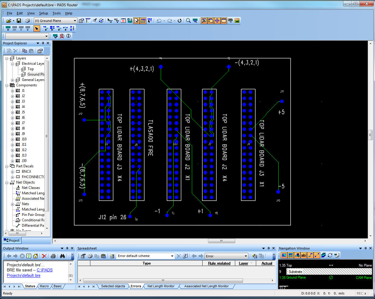
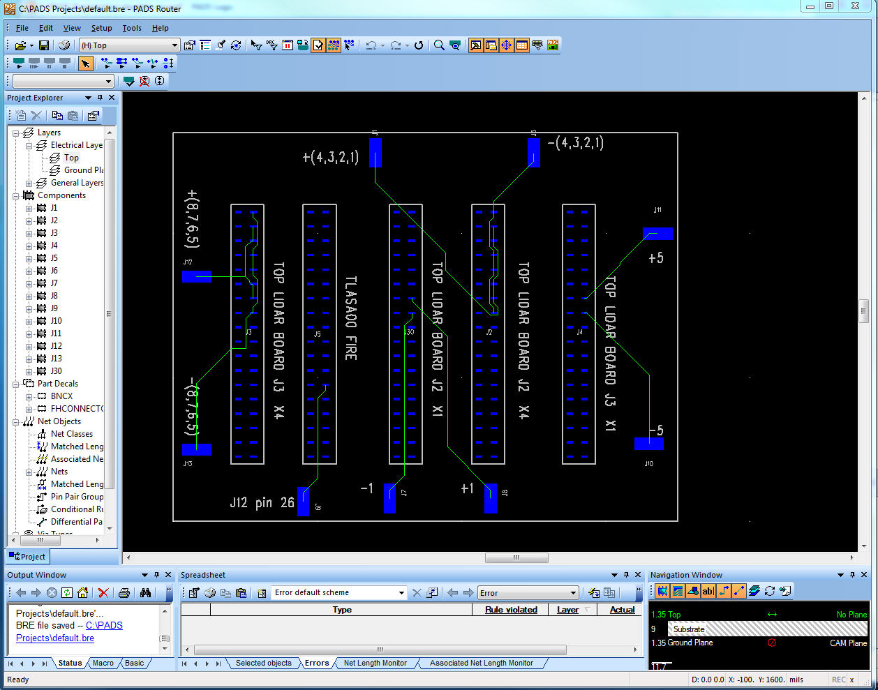
I have a very, very simple two layer board (see attached).
My initial question is why is it that my ground plane looks so similar to my top plane? I specified my 2nd layer to be a ground plane so I was expecting my signals to be only seen on the top layer. But it looks like my signals are both on top and bottom.
Just starting doing my own pcb design. So if you need to see a different file just let me know.