muffassir
Member level 3

- Joined
- Sep 15, 2011
- Messages
- 67
- Helped
- 10
- Reputation
- 20
- Reaction score
- 10
- Trophy points
- 1,288
- Location
- Planet Earth
- Activity points
- 1,802
Hi all,
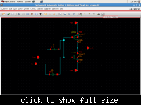
Please refer my inverter ckt in the attachment (scematics.png). i am designing the floating Gate programmable inverter.So by panning thru a lot of IEEE papers i have been able to design this inverter.
So in my inverter i am using two capacities Cin =1pF and Ctun=1pF. Nmos anf PMOS are of same sizes for 180nm technology.
NOTE:Ctun and Vtun is used to tunnel out the electrons that are trapped between the two gates..i.e tunneling of electrons concept
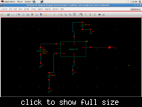
see test_schematic attachment for the test ckt. Wherein Vpulse is the Vin to the inverter with v1=0v, v2=1.8v , td=0 ,tr=tf=1ns and ton=10n T=20n ,,vdc=1.8v ,,,Vtun=5V..
I have done the trans and DC analyses of the above ckt with trans of stop time of 200ns and DC for sweep range of 0 to 1.8
see the attachment output for the ADE window...here you can see the trans and DC outputwaveforms ....
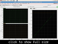
in TRANS analysis the input is properly inverted to give the output signal ...
BUT the DC analysis fails to give the expected VTC curve of the inverter( i am getting straight line of 1.8v)..WHY??
How can i get the VTC curve ...where i am going wrong in the analysis please point it out....
Thanks in advance!!
Please refer my inverter ckt in the attachment (scematics.png). i am designing the floating Gate programmable inverter.So by panning thru a lot of IEEE papers i have been able to design this inverter.
So in my inverter i am using two capacities Cin =1pF and Ctun=1pF. Nmos anf PMOS are of same sizes for 180nm technology.
NOTE:Ctun and Vtun is used to tunnel out the electrons that are trapped between the two gates..i.e tunneling of electrons concept

see test_schematic attachment for the test ckt. Wherein Vpulse is the Vin to the inverter with v1=0v, v2=1.8v , td=0 ,tr=tf=1ns and ton=10n T=20n ,,vdc=1.8v ,,,Vtun=5V..
I have done the trans and DC analyses of the above ckt with trans of stop time of 200ns and DC for sweep range of 0 to 1.8

see the attachment output for the ADE window...here you can see the trans and DC outputwaveforms ....

in TRANS analysis the input is properly inverted to give the output signal ...
BUT the DC analysis fails to give the expected VTC curve of the inverter( i am getting straight line of 1.8v)..WHY??
How can i get the VTC curve ...where i am going wrong in the analysis please point it out....
Thanks in advance!!
Last edited:
