Continue to Site

Welcome to EDAboard.com

Welcome to our site! EDAboard.com is an international Electronics Discussion Forum focused on EDA software, circuits, schematics, books, theory, papers, asic, pld, 8051, DSP, Network, RF, Analog Design, PCB, Service Manuals... and a whole lot more! To participate you need to register. Registration is free. Click here to register now.

two-stage OP DC voltage at its inputs: presim versus post-sim

Status
Not open for further replies.

allennlowaton

Full Member level 5
Full Member level 5
Joined
Oct 5, 2009
Messages
247
Helped
3
Reputation
6
Reaction score
3
Trophy points
1,298
Location
Taiwan
Activity points
3,081
I did a post-simulation with my OP alone. I found out that there's a 20mV~30mV DC difference on its inputs. The gain is not anymore positive. Further simulation shows that the said OP can only afford to have 2mV DC difference on its inputs. How can I improved my OP to obtain such requirement?

---------- Post added at 09:34 ---------- Previous post was at 07:52 ----------

this is the circuit in which the post-sim results being obtained from
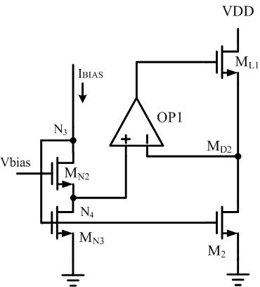
65_1320741272.jpg
 

How did you match the MN3 and M2?
How did you match the input differential transistor of the OP1?
 
I only showed M2 in the figure, as a matter of fact there are other three branches (M3, M4, and M5) in my circuit.
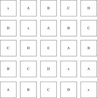
With that I used this matching style;


For the input pairs of the OP1, I used

AB
BA
 

I'm confused about the circuit. It shouldn't be so much mismatch with this matching style.
So i think you should check the OP1. Is the gain or driving force of the OP1 enough?
As your picture shown, the ML1 is used as power mos. isn't it?
So i think it's large amount of mosfet.
 
Last edited:
I checked the post simulation of a stand-alone OP, when the difference of the DC inputs ranges from 20mV~30mV. The gain is already negative. How can I improved my OP? ML1's device size is 500u.
 

I checked the post simulation of a stand-alone OP, when the difference of the DC inputs ranges from 20mV~30mV. The gain is already negative.

The gain is negative just because the input voltage has 20mV~30mV difference.
please tell me the structure and the bias current of the OP1.
And you can add a cap to your schematic between the OP1 output and the gate of ML1, which is about 5~10pf. Then you can run a simulation, tell me the result.
 
Last edited:
I don't have a problem during the PRESIM. The 20mV~30mV difference has been found on the POST-SIM.
The OP is a two-stage and the bias current is 4uA.
 

Status
Not open for further replies.

Part and Inventory Search

Welcome to EDABoard.com

Sponsor

Back
Top